
Gate-Tunable Graphene Josephson Junctions for Terahertz Detection
Researchers demonstrate a gate-tunable graphene Josephson junction, creating a highly sensitive and adaptable detector for terahertz frequencies. Learn how...
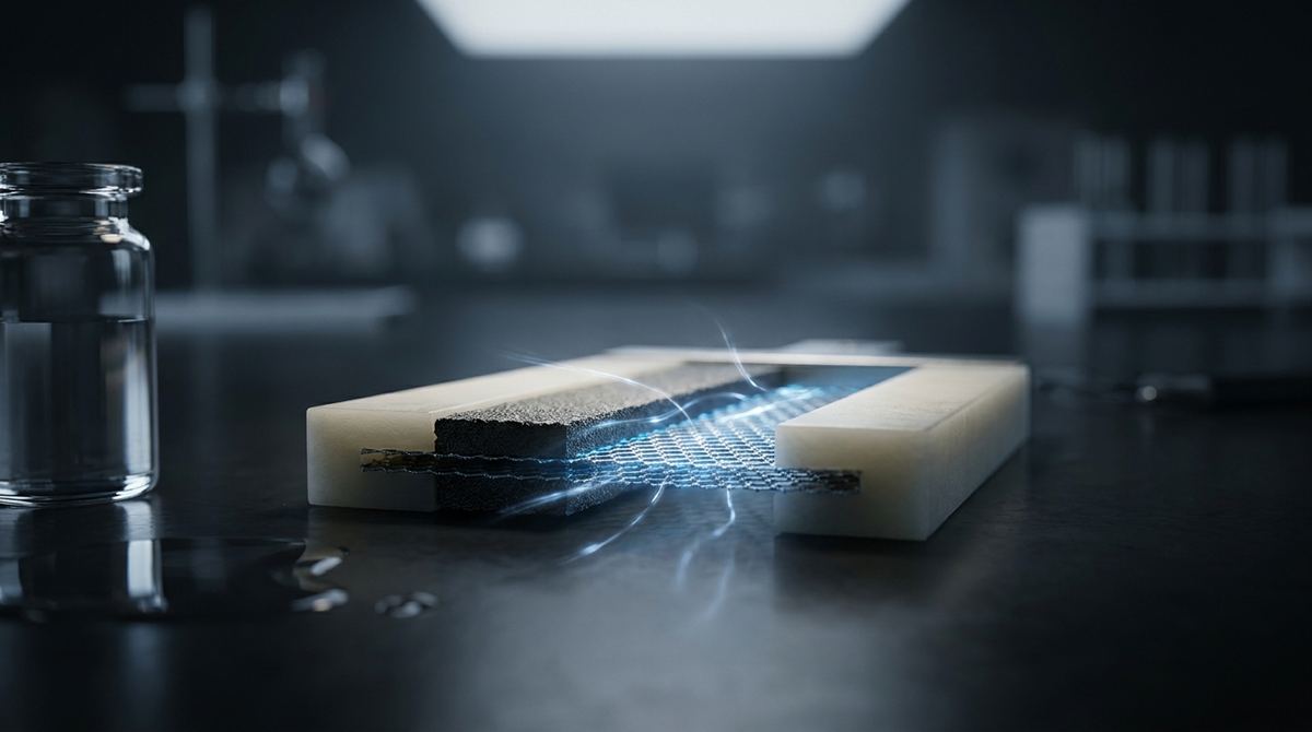
The relentless pace of technological advancement is fundamentally limited by the speed at which we can manipulate electrons in materials. For decades, silicon has been the undisputed champion, but as we push toward terahertz frequencies for communications and computing, we are approaching silicon's physical limits. The challenge is no longer just about making components smaller, but about making them faster and more efficient. This requires a deeper understanding of how charge carriers—the electrons and holes that constitute an electrical current—behave on incredibly short timescales, measured in quadrillionths of a second. New materials like graphene offer tantalizing possibilities, but unlocking their full potential requires a new set of rules. Groundbreaking research is showing that the key to controlling graphene's electronic properties might not lie within the material itself, but in the environment that surrounds it.
In any electronic material, when energy is introduced—for instance, from a pulse of light or an electric field—it excites the charge carriers, creating what are known as "hot carriers." These energized electrons and holes are the lifeblood of high-speed devices. However, they lose their excess energy very quickly, typically by colliding with the atomic lattice of the material and dissipating it as heat (vibrations called phonons). This process, known as carrier scattering and cooling, is a fundamental bottleneck. If carriers cool too quickly, the signal is lost before it can be processed. If they generate too much heat, the device becomes inefficient and can fail. This is the central challenge that a team of researchers, including Hai I. Wang, Xiaoyu Jia, Anand Nivedan, Mischa Bonn, Aron W. Cummings, Alessandro Principi, and Klaas-Jan Tielrooij, set out to address. Their work explores how to precisely control these ultrafast energy-loss pathways in graphene. The goal is to develop a method to either accelerate or slow down carrier cooling on demand, effectively tuning the material's properties for a specific task.
The central insight of this research is that the material placed directly underneath a sheet of graphene is not just a passive support structure. Instead, this underlying substrate can actively influence and control the behavior of electrons within the graphene layer. The team investigated the use of dielectric materials as substrates. A dielectric is an electrical insulator, but its constituent atoms can form electric dipoles when subjected to an electric field. The researchers hypothesized that the atomic vibrations (phonons) within the dielectric substrate could interact with the hot carriers in the graphene layer above it through long-range electrical forces. This interaction, known as remote phonon scattering, provides a new, external pathway for the hot electrons in graphene to shed their energy. By carefully selecting a dielectric substrate with specific vibrational properties, they could essentially open up a custom-designed energy drain for the graphene. Conversely, by choosing a different substrate, they could close off this pathway, forcing the carriers to remain "hot" for much longer. In essence, the researchers have demonstrated a way to use the substrate as a tuning knob for the ultrafast thermodynamics of graphene's electrons.
The experimental approach to studying these fleeting phenomena is a marvel of precision. The researchers used a technique called optical pump-terahertz probe (OPTP) spectroscopy. This method allows them to observe the state of electrons on femtosecond (a millionth of a billionth of a second) timescales. The setup involves preparing a high-quality single layer of graphene and transferring it onto different dielectric substrates, such as silicon dioxide or hexagonal boron nitride. An intense, ultrashort "pump" laser pulse is fired at the graphene sample. This pulse acts like a flash of energy, instantly creating a population of hot carriers. Immediately afterward, a much weaker "probe" pulse, in the terahertz frequency range, is sent through the sample. The amount of the terahertz probe that is absorbed by the graphene is directly related to its conductivity, which in turn depends on the state of its charge carriers. By precisely varying the time delay between the pump and the probe pulses, from femtoseconds to picoseconds, the team could create a stop-motion movie of how the graphene's conductivity changes as its hot carriers cool down. By repeating this experiment on graphene samples placed on different dielectric substrates, they could directly compare the cooling dynamics and isolate the specific influence of each underlying material.
The results provided clear and compelling evidence for their hypothesis. The researchers discovered that the cooling rate of hot carriers in graphene was dramatically different depending on the dielectric substrate it was placed on. They observed that when graphene was on a substrate whose phonon energies were resonant with the energy of the hot carriers, a highly efficient cooling channel was established. The energy from the excited electrons in the graphene was effectively and rapidly transferred into the atomic vibrations of the substrate. This led to a very fast return to the material's equilibrium state. In contrast, when graphene was placed on a substrate with phonon energies that were not well-matched to the carrier energies, this remote scattering pathway was suppressed. In this case, the hot carriers remained energized for a significantly longer period, as they were forced to rely on slower, intrinsic cooling mechanisms within the graphene itself. This finding demonstrates unequivocally that the dielectric environment is an active and powerful tool for engineering the non-equilibrium properties of graphene. It validates the concept of "dielectric control" as a viable strategy for manipulating ultrafast carrier dynamics.
This discovery is significant because it provides a new degree of freedom for designing graphene-based devices. Until now, efforts to modify graphene's properties have largely focused on intrinsic methods like chemical doping, strain engineering, or creating nanostructures. These methods can be effective but are often permanent and can introduce defects that degrade the material's exceptional electronic quality. Dielectric control, on the other hand, is a non-invasive, passive technique. Engineers can now think about the substrate not just as a mechanical support but as an integral part of the electronic circuit. For applications like photodetectors, where the goal is to convert light into a lasting electrical signal, one would choose a substrate that minimizes remote phonon scattering, thereby prolonging the lifetime of hot carriers and increasing the chance of their collection. For applications in high-speed optical modulators, the opposite is desired. A substrate that promotes rapid cooling would allow the device to be switched on and off at much higher frequencies. This research provides a foundational design principle for a new generation of graphene electronics and photonics devices where performance is tuned through environmental engineering.
While this work represents a major step forward, it is important to recognize its context as fundamental laboratory research. The experiments were conducted on small, pristine flakes of graphene under controlled conditions. Translating these findings to commercially viable technology will require overcoming several hurdles. A primary challenge is the scalability of high-quality materials. The delicate energy transfer mechanisms observed depend on a clean and uniform interface between the graphene and the substrate. Any impurities, wrinkles, or defects could disrupt the process. Advances in scalable graphene production will be critical to achieving these ideal interfaces over large, wafer-scale areas. Furthermore, the study focused on a limited set of dielectric substrates. A comprehensive library of materials and their corresponding effects on graphene's carrier dynamics needs to be developed to give engineers a full palette of options. Finally, real-world devices include metallic contacts, gating electrodes, and encapsulation layers, all of which will introduce additional interfaces and potential scattering pathways that must be understood and accounted for in a complete device model.
The ability to precisely control carrier lifetimes in graphene opens doors to a wide range of advanced technologies. The most immediate impact is expected in the field of terahertz (THz) science and technology. The THz gap, lying between conventional electronics and photonics, is the frontier for next-generation wireless communications (6G and beyond), high-resolution security screening, and medical imaging. Graphene is a uniquely promising material for building active THz components like modulators, switches, and detectors. This research provides a clear roadmap for optimizing graphene's response time for these demanding applications. Another key area is optoelectronics. More efficient photodetectors, particularly in the infrared spectrum, could be developed by using substrates that extend carrier lifetimes, boosting the signal generated from incoming photons. This same principle could enhance the efficiency of novel solar energy harvesting devices, allowing them to capture more of the sun's energy before it is lost to heat. The broad portfolio of potential graphene applications in sensing, energy, and communications will all benefit from this deeper understanding of how to engineer its fundamental electronic behavior.
If there is one key takeaway from this pioneering work, it is this: the material directly underneath a sheet of graphene is not just a stage, but an active participant in its electronic performance. By intelligently choosing the substrate, we can control the energy and lifetime of electrons within graphene on ultrafast timescales, providing a powerful new method for designing the next generation of high-speed electronic and optoelectronic devices.
What is a dielectric material?
A dielectric is a type of material that is an electrical insulator, meaning it does not conduct electricity well. However, when placed in an electric field, its internal charges can shift slightly, creating tiny electric dipoles. This ability to be polarized allows it to store energy and, as this research shows, to interact with charge carriers in adjacent materials through electric fields without direct contact.
What are "hot carriers" in graphene?
In a material like graphene at rest, electrons occupy the lowest available energy states. When energy is suddenly added, for instance from a laser pulse, these electrons are kicked into much higher energy states. These highly energized electrons and their corresponding positive charges (holes) are referred to as "hot carriers." They are not in thermal equilibrium with the material's atomic lattice and will rapidly cool down by shedding this excess energy.
Why is controlling "ultrafast" carrier dynamics important for electronics?
The speed at which carriers cool down and return to their resting state determines the fundamental speed limit of an electronic device. For a transistor to switch or a photodetector to register a signal, it must be able to reset itself before the next bit of information arrives. By controlling dynamics on ultrafast (femtosecond to picosecond) timescales, we can design components that operate at terahertz frequencies, enabling data transmission and processing speeds thousands of times faster than today's technology.
Does this research mean we will have graphene computers next year?
No, this is a foundational scientific discovery, not a market-ready product. It reveals a new physical principle for designing graphene devices. Significant engineering challenges remain in scaling up production, ensuring material quality and interface purity, and integrating these concepts into complex circuits. This work provides the scientific blueprint that engineers will use to develop future technologies over the next decade.
How is this "dielectric control" different from traditional doping of graphene?
Traditional doping involves introducing chemical impurities or applying a static electric field to permanently change the number of free charge carriers (electrons or holes) in graphene, which primarily affects its baseline conductivity. Dielectric control, as described here, does not change the number of carriers. Instead, it influences their dynamic behavior after they have been excited, controlling how quickly they lose energy. It is a tool for managing the transient, high-energy state of the material, which is crucial for high-speed applications.
The work by Hai I. Wang and his collaborators provides a profound insight into the physics of graphene and a practical tool for the engineers of tomorrow. By demonstrating that the dielectric environment can be used to dictate the ultrafast energy pathways of charge carriers, they have moved the field beyond manipulating the material in isolation. This research establishes the principle of substrate-based environmental engineering as a powerful, non-invasive strategy to tailor the properties of two-dimensional materials. It lays the scientific groundwork for designing a new class of graphene-based devices optimized for the unprecedented speeds required by future communication and computing paradigms. The path from the laboratory to industrial application is long, but this discovery illuminates a clear and promising direction forward.
Serious about B2B integration? Test our premium Pulsed Electrical Resistive Carbon Heating turbostratic graphene in your lab. 100g sample packs available now.
Explore More
Researchers demonstrate a gate-tunable graphene Josephson junction, creating a highly sensitive and adaptable detector for terahertz frequencies. Learn how...

Researchers reveal how breaking inversion symmetry in 2D metals enables electronic Raman scattering, a powerful, non-destructive tool for characterizing...

Researchers use AI to accelerate the discovery of new materials, identifying a graphene-boron nitride composite for interstellar spacecraft shielding.