
AI Designs Graphene Nanocomposite for Interstellar Spacecraft Shielding
Researchers use AI to accelerate the discovery of new materials, identifying a graphene-boron nitride composite for interstellar spacecraft shielding.
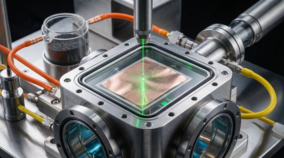
Imagine trying to understand a complex engine just by listening to it run. The main hum tells you it’s on, but the subtle clicks, whirs, and resonances reveal how the individual components are performing. For materials scientists, characterizing the electronic properties of advanced materials like graphene is a similar challenge. Standard tools can hear the main hum, but they often miss the subtle details that are critical for building next-generation electronics. A new theoretical breakthrough, however, offers a way to listen to the quantum whispers of these materials, providing a far richer understanding of their inner workings.
The promise of two-dimensional (2D) materials, from graphene to transition metal dichalcogenides (TMDs), hinges on our ability to precisely understand and control their electronic behavior. Every future application, whether it's a faster transistor, a more sensitive photodetector, or a more efficient solar cell, depends on the intricate dance of electrons within that atomically thin layer. The challenge lies in observing this dance without disturbing it. Many characterization techniques are destructive, require cryogenic temperatures, or provide only an averaged-out picture of the material’s properties.
One of the most powerful non-destructive tools available is Raman spectroscopy. It involves shining a laser on a material and analyzing the light that scatters off. This technique is exceptionally good at detecting the vibrations of the crystal lattice, known as phonons, which provides a structural fingerprint of the material. However, using it to directly probe the electrons themselves, the very heart of the material's electronic function, is far more difficult. In many highly symmetric materials like pristine graphene, the fundamental rules of quantum mechanics forbid certain electronic transitions from appearing in the Raman signal. This means that a wealth of valuable information remains hidden from view. The theoretical work by researchers Mojdeh Saleh and Saurabh Maiti provides a key to unlock this hidden information.
At the core of this research is the concept of symmetry. Think of a perfectly symmetrical butterfly. If you reflect its left side across the center, you get a perfect copy of its right side. Many crystals have a similar property called inversion symmetry. This means that if you take any point in the crystal and flip it through a central origin point, you will land on an identical atom. A single, perfect sheet of graphene possesses this inversion symmetry. This symmetry imposes strict "selection rules" on how light can interact with the material's electrons, effectively silencing certain signals.
The key insight from Saleh and Maiti is that if you intentionally break this inversion symmetry, you change the rules of the game. You can break this symmetry in several ways: by stacking two layers of graphene and applying an electric field, which makes the top and bottom layers electronically different, or by using a 2D material like molybdenum disulfide (MoS2) that naturally lacks this symmetry in its structure. When inversion symmetry is broken, the previously "forbidden" electronic signals become "allowed." This means that electronic Raman scattering (ERS), a technique that was once blind to these features, can suddenly see them. In essence, the researchers have found a way to switch on a new light source in a previously dark room, illuminating the electronic properties of these materials with unprecedented detail.
To understand how this works, we must first look at the process of Raman scattering on a quantum level. When a photon of light from a laser strikes a material, it can excite an electron, kicking it to a higher energy level. The electron then falls back, and the material emits a new photon. Most of the time, the emitted photon has the exact same energy as the incoming one. But occasionally, the electron doesn't fall back to its original state, leaving some of the photon's energy behind in the material as an excitation. The scattered photon therefore leaves with slightly less energy, and this energy difference is the Raman signal.
In electronic Raman scattering, the excitation left behind is purely electronic; an electron has been moved from one energy state to another. The specific "jumps" an electron can make are dictated by the material's electronic band structure and the quantum mechanical selection rules. In a 2D metal with inversion symmetry, the interaction between the light and the electrons is constrained, and many potential jumps are forbidden.
Saleh and Maiti's theoretical framework models what happens when that symmetry is gone. Their calculations show that in a material with broken inversion symmetry, the light can couple to the electrons in new ways. This opens up new channels for ERS, particularly for what are known as "intraband" transitions, where electrons are excited to a higher energy state within the same electronic band. These signals, which are directly related to the material's ability to conduct electricity, are normally invisible in symmetric systems. By breaking the symmetry, these signals emerge in the Raman spectrum as a broad continuum at low energy shifts, a feature whose precise shape and intensity are a direct signature of the material's metallic character and electronic structure. This detailed understanding is foundational for creating reliable graphene electronics.
The work of Saleh and Maiti is theoretical, meaning they used mathematical modeling to predict what an experiment should find. They calculated the expected ERS spectrum for a model 2D metallic system where inversion symmetry was broken. Their primary finding is a clear, quantitative prediction of a new feature that should appear in the Raman spectrum. This feature is not just a simple peak; it's a broad signal whose characteristics are directly tied to the fundamental electronic properties of the material.
They established a direct mathematical link between the shape of this new Raman signal and parameters like the Fermi energy (which describes the energy level of the most energetic electrons) and the electron scattering rate (which relates to the material's conductivity). In essence, they have created a translation guide. An experimentalist can measure the specific shape of the ERS signal, and by using the formulas derived by Saleh and Maiti, can directly calculate these critical electronic parameters. This provides a new spectroscopic fingerprint that not only identifies the material's state but quantifies it with high precision.
This research is significant because it proposes a new, powerful, all-optical, and non-destructive method for characterizing some of the most promising materials for future technology. The ability to accurately measure the electronic properties of 2D materials is a major bottleneck in both research and manufacturing. This theoretical work provides a roadmap for turning a common piece of laboratory equipment, the Raman spectrometer, into a much more profound diagnostic tool.
For manufacturing, this could be a game-changer. Imagine a quality control system on a production line that uses this technique to scan sheets of a 2D material. It could instantly map out variations in electronic properties, flagging defects or inconsistencies that would be invisible to other methods. Ensuring this level of uniformity is essential for producing a reliable industrial graphene supply for high-performance applications. For scientists in research and development, it accelerates the discovery cycle. Instead of relying on more complex and time-consuming techniques, they could rapidly screen new materials or test the effects of different fabrication processes, dramatically speeding up the path from concept to functional device.
It is crucial to remember that this is a theoretical study. The predictions, while rigorously derived, now need to be confirmed through careful experiments. This will be a non-trivial task. The predicted ERS signals from electrons are often much weaker than the signals from lattice vibrations (phonons), and experimentalists will need to devise clever ways to isolate and accurately measure these faint electronic whispers from the loud phononic shouts.
Furthermore, the model used by the researchers is an idealized one. Real-world materials are never perfect; they contain defects, impurities, and strain, and they sit on substrates that can influence their behavior. Each of these imperfections can complicate the Raman spectrum. The next steps will involve both experimental validation of the core idea and further theoretical work to understand how these real-world non-idealities will affect the ERS signal. Translating this from a laboratory proof-of-concept to a robust industrial tool suitable for integration with graphene production machinery will require significant future research and engineering.
The most immediate application of this work is in the field of metrology, the science of measurement, for the semiconductor industry. As companies work to build transistors, sensors, and optical components out of 2D materials, they need reliable ways to verify that the material meets precise electronic specifications. This technique could provide that verification.
For example, in a field-effect transistor made from bilayer graphene, the size of the band gap is controlled by an external electric field. This technique could allow for a direct, in-operando measurement of that band gap, providing critical feedback for device design and optimization. It could also be used to characterize the quality of electrical contacts between metals and 2D materials, a persistent challenge in nanoelectronics. Ultimately, by providing a clearer window into the electronic world of 2D materials, this work will help accelerate the development of a wide range of graphene applications, from ultra-high-frequency communication systems to highly sensitive biosensors.
By strategically breaking a 2D material's natural symmetry, scientists can unlock previously hidden information about its electronic properties. This allows a common measurement tool, Raman spectroscopy, to be used in a new and much more powerful way, providing a direct window into the quantum behavior that governs next-generation devices.
What is Raman scattering?
Raman scattering is a non-destructive technique that uses a laser to probe a material. Think of it like tapping a bell with a hammer and listening to the sound it makes. The specific "tone" or frequency of the scattered light gives scientists detailed information about the material's atomic vibrations and, in some cases, its electronic properties.
What is inversion symmetry in a material?
Inversion symmetry is a property of a crystal's atomic arrangement. Imagine a perfectly symmetrical snowflake; if you could flip it through its center point, it would look exactly the same. Materials with this property have very orderly structures that impose strict rules on how particles like electrons and photons can interact within them.
Why is breaking this symmetry important for this research?
Breaking the inversion symmetry fundamentally changes the quantum mechanical "rules" inside the material. It makes certain interactions between light and electrons, which were previously forbidden, become allowed. This allows researchers to see new signals using techniques like Raman spectroscopy, revealing information that was previously invisible.
Is this a new material or a new measurement technique?
This research does not introduce a new material but rather a new theoretical framework for using an existing measurement technique, Raman spectroscopy, in a more powerful way. It's a new recipe that tells scientists how to unlock more information from a class of materials they are already studying.
What is the difference between probing phonons and electrons with Raman?
Probing phonons, or lattice vibrations, tells you about the physical structure and rigidity of the material, like checking the frame and chassis of a car. Probing electrons tells you about the material's electrical and optical properties, which is like analyzing the performance of the engine and electronics. Both are important, but probing electrons is more directly related to the material's function in an electronic device.
The theoretical work by Mojdeh Saleh and Saurabh Maiti provides an elegant and insightful blueprint for advancing our understanding of 2D metals. By demonstrating how the deliberate breaking of inversion symmetry can activate dormant electronic signals in Raman spectroscopy, they have outlined a path toward a powerful new characterization tool. This bridge between fundamental quantum theory and practical materials science is essential for progress. While experimental verification remains the critical next step, this research illuminates a promising new direction for probing, understanding, and ultimately engineering the remarkable 2D materials that will define the future of technology.
Serious about B2B integration? Test our premium Pulsed Electrical Resistive Carbon Heating turbostratic graphene in your lab. 100g sample packs available now.
Explore More
Researchers use AI to accelerate the discovery of new materials, identifying a graphene-boron nitride composite for interstellar spacecraft shielding.

In BN-encapsulated graphene, the ultimate limit on electron speed is not graphene itself, but remote phonon scattering from the insulating layers that...

Determinant Monte Carlo simulations are key to materials science but fail at low temperatures. New research offers a stable algorithm, enabling accurate...