
Elasticity Reshapes Heat Flow in Graphene
New research reveals that mechanical strain doesn't just reduce but fundamentally reshapes heat flow in graphene, a critical insight for flexible...
The characterization of 2D materials like graphene is a foundational step in developing next-generation electronics and sensors. For small labs and startups, the go-to method is often DC transport measurement, which involves passing a current through the material and measuring its resistance. While effective, this technique has a significant drawback: it is highly sensitive to microscopic imperfections. A single crack, a poorly-made contact, or a region of disorder can create a bottleneck for current, dominating the measurement and masking the true electronic properties of the bulk material.
This guide presents a practical alternative based on recent research: gate reflectometry. It is a non-contact, radio-frequency (RF) technique that measures the quantum capacitance of a material. This approach provides a more holistic view of the material's electronic state, effectively averaging over small defects. It is less susceptible to the percolation issues that plague DC transport, giving you a cleaner, more reliable picture of your sample's quality and behavior.
We will walk through the design, construction, and testing of a gate reflectometry setup for characterizing bilayer graphene heterostructures. This project is based on the methodology demonstrated by Tamás Kalmár et al. in their 2026 paper, "Capacitance sensing in bilayer graphene with gate reflectometry." This powerful technique can be scaled for material quality control and is an invaluable tool for exploring the complex physics of van der Waals heterostructures. For more on how graphene is enabling new technologies, see our articles on graphene sensors.
At its core, gate reflectometry works by turning your 2D material device into part of a sensitive radio resonator. Imagine an LC tank circuit, the simple combination of an inductor (L) and a capacitor (C) that resonates at a specific frequency. In our setup, we intentionally create such a circuit, but with a twist: the device's top gate and the graphene layer itself act as one of the capacitors.
The key insight is that the capacitance of the graphene layer is not constant. It changes based on its electronic state, a property known as quantum capacitance. By applying a DC voltage to the gates, we can fill or empty electronic states in the graphene, which in turn changes this quantum capacitance.
This change, however small, alters the total capacitance of the LC circuit. A change in capacitance causes a shift in the circuit's resonance frequency. We can detect this tiny frequency shift with high precision using an RF measurement technique called reflectometry.
Here is the process:
1. An LC resonator is coupled directly to the top gate of the graphene device.
2. A stable, single-frequency RF signal is sent to the resonator. This frequency is chosen to be on the steep slope of the resonator's resonance curve, where the system is most sensitive to changes.
3. We measure the signal that is reflected from the resonator.
4. As we apply DC voltages to the device's gates to manipulate the graphene's electronic state, its quantum capacitance changes.
5. This capacitance change shifts the resonance frequency, which alters how much of the RF signal is reflected.
6. By recording the reflected signal's power or phase, we create a high-resolution map of the material's quantum capacitance as a function of its carrier density and electric field.
This RF signal provides a robust, non-invasive probe of the material's fundamental electronic density of states, bypassing the issues of contact resistance and local defects.
Building this setup requires components for the device itself, the resonator circuit, and the measurement hardware.
Device Under Test (DUT):
Bilayer Graphene (BLG): High-quality exfoliated or CVD-grown bilayer graphene is the active material. While the source paper focuses on bilayer, this technique could be adapted for other 2D materials. You can source high-purity turbostratic graphene flakes for exfoliation.
Substrate: A standard silicon wafer with a thermally grown silicon dioxide layer (e.g., Si/SiO₂ 285 nm) serves as the substrate and the global back gate.
Encapsulation Materials: Hexagonal boron nitride (hBN) is used as an atomically flat, insulating dielectric to encapsulate the graphene, preserving its high mobility. The source also includes tungsten diselenide (WSe₂) to induce strong spin-orbit coupling, a step relevant for topological state research.
Electrodes: Metal contacts for source, drain, and the top gate are required. Typically, a stack like Chromium/Gold (Cr/Au, e.g., 5 nm/50 nm) is used.
Resonator Components:
Chip Inductor: A surface-mount device (SMD) inductor forms the 'L' of the LC circuit. The source paper's design implies an inductance around 390 nH to achieve resonance near 1.1 GHz. This is a good starting value.
Parasitic Capacitance: The 'C' is primarily formed by the parasitic capacitance of the top gate electrode, the wire bond, and the PCB pad. This is not a discrete component but an inherent part of the design.
Measurement Hardware:
Printed Circuit Board (PCB): A custom PCB designed for RF signals is needed to mount the device chip and the resonator components.
RF Connectors and Cabling: High-frequency SMA connectors and low-loss coaxial cables are essential.
Bias Tee: This crucial component allows you to combine the low-frequency DC gate voltage with the high-frequency RF probe signal onto a single coaxial line.
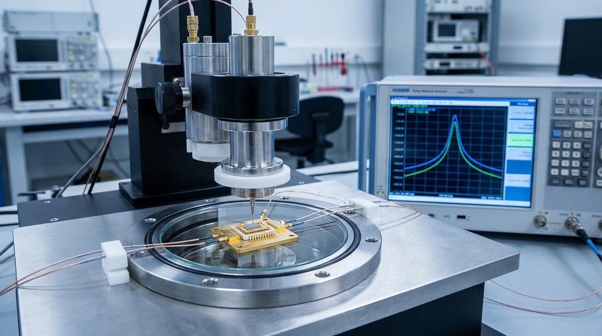
Vector Network Analyzer (VNA): A VNA is the ideal instrument for characterizing the resonator and measuring the reflected RF signal (the S11 parameter). A simpler setup with a dedicated RF signal generator and a power detector or spectrum analyzer could also work.
Low-Noise DC Voltage Source: A precision voltage source is needed to apply bias to the top and back gates.
Cryogenic Probe Station: To observe the quantum capacitance effects clearly and reduce thermal noise, the measurements must be performed at low temperatures (e.g., liquid helium temperature, ~4 Kelvin).
Fabricating the van der Waals heterostructure is the most challenging part of this project, requiring cleanroom access and specialized equipment.
1. Substrate Preparation: Begin with a clean Si/SiO₂ wafer. This will act as your global back gate.
2. Material Exfoliation: Use the standard mechanical exfoliation technique ("Scotch tape method") to obtain atomically thin flakes of graphene, hBN, and WSe₂ from bulk crystals.
3. Stack Assembly: Using a microscope-equipped transfer stage, assemble the heterostructure layer by layer. A common stacking order, following the source paper's device, is bottom hBN, WSe₂, bilayer graphene, and finally top hBN. This encapsulates the active layers, protecting them from contamination.
4. Device Patterning: Use electron-beam lithography (EBL) or photolithography to define the device geometry, such as a Hall bar shape. A subsequent plasma etch (e.g., with CHF₃/O₂) removes the unwanted material.
5. Contact and Gate Deposition: Use a second lithography step to define the areas for the source/drain contacts and the top gate. Deposit the contact metal (e.g., Cr/Au) using an evaporator, followed by a lift-off process.
This fabrication process is complex and requires significant expertise. For more background on material synthesis and processing, you can explore resources on graphene manufacturing techniques.
With the device chip fabricated, the next step is to integrate it into the RF resonator circuit.
1. PCB Design: Design a small PCB, preferably on an RF-grade substrate like Rogers 4350B, though standard FR-4 can work for initial tests. The design should include a 50-ohm coplanar waveguide trace leading from an SMA connector to the device area. Include pads for the device chip, the SMD inductor, and DC input lines with sufficient filtering capacitors.
2. Component Assembly: Solder the SMA connector and any bias-tee components onto the PCB.
3. Resonator Integration: Mount the 390 nH SMD inductor on the PCB. One end connects to the RF signal line, and the other end connects to a pad designated for the top gate connection.
4. Chip Mounting and Wire Bonding: Securely mount your fabricated graphene device chip onto the PCB. Using a wire bonder, create a short, direct connection from the top gate pad on your chip to the inductor pad on the PCB. This connection is critical; its length contributes to the total inductance and capacitance. Bond the other required pads (source, drain, back gate) to their respective lines on the PCB.
The quality of this assembly directly impacts the resonator's performance, specifically its quality factor (Q-factor). A high Q-factor results in a sharper resonance and thus higher measurement sensitivity.
Once the device is mounted and wired inside your cryogenic probe station, you can begin the characterization process.
1. Find the Resonance: Cool the system down to its base temperature. Connect the VNA to the PCB's SMA connector and perform a one-port reflection measurement (S11). Sweep the frequency, for instance, from 500 MHz to 2 GHz. You are looking for a sharp dip in the reflected power (a dip in the S11 magnitude plot). This is your circuit's resonance frequency, f₀. With a 390 nH inductor, this should be around 1-1.2 GHz. Record this frequency and the Q-factor of the resonance.
2. Establish a DC Baseline: Before the RF measurement, perform a standard DC transport test. Sweep the top gate (V_tg) and back gate (V_bg) voltages while measuring the two-terminal or four-terminal resistance of the graphene device. This will generate a resistance map that shows features like the main charge neutrality point. This map will serve as a valuable comparison for your reflectometry data.
3. Perform Gate Reflectometry:
Set the VNA to a fixed frequency. For maximum sensitivity, choose a frequency on the steepest part of the resonance curve's slope, slightly detuned from f₀.
Configure your VNA to measure the magnitude or phase of the reflected signal (S11) over time.
Using your DC voltage sources, perform the same two-dimensional sweep of V_tg and V_bg that you did for the DC measurement.
At each (V_tg, V_bg) point, record the value of the reflected RF signal.
4. Analyze the Data:
Create a 2D color plot of the reflected RF signal as a function of V_tg and V_bg.
Compare this RF map to your DC resistance map. You should see corresponding features, especially the main charge neutrality point.
The key result from the source paper is that the RF signal can clearly show the opening of a band gap in the bilayer graphene as a large, uniform feature. In the DC resistance map, this same feature might appear noisy or fragmented due to charge puddles and percolating channels. The RF measurement's robustness to this disorder is its primary advantage.
If your hBN and graphene layers are rotationally aligned, you may also see secondary features corresponding to a moiré superlattice, which this technique can resolve beautifully.
This powerful method provides a direct window into the electronic structure of your material, making it a cornerstone for advanced graphene electronics research.
Low Device Yield: Van der Waals heterostructure fabrication is notoriously difficult. Mitigation: Maintain strict cleanroom protocols. Practice with less critical materials. Fabricate multiple devices in parallel to increase the chance of getting a high-quality sample.
Poor Resonator Performance: A low Q-factor will result in poor measurement sensitivity. Mitigation: Use a high-Q inductor. Keep wire bonds as short as possible. Use a well-designed RF PCB with proper impedance matching and grounding.
RF Interference and Noise: The small signals can be easily buried in noise. Mitigation: Ensure all cabling is properly shielded. Use low-noise DC sources and amplifiers. Proper grounding of all equipment within the cryogenic setup is critical.
Complex Data Modeling: Extracting the absolute quantum capacitance value in Farads requires a comprehensive circuit model that accounts for all parasitic elements. Mitigation: For initial characterization, focus on the qualitative changes in the reflected signal. The relative change is often the most important data, clearly indicating band gap openings, phase transitions, or other electronic phenomena.
This guide is based on the methods presented by Kalmár et al. (2026). The core concept of using a lumped-element LC resonator coupled to a top gate for capacitance sensing is directly from this work. The use of a BLG/hBN/WSe₂ heterostructure and the comparison of RF reflectometry to DC transport are central findings of the paper.
Certain practical details are engineering assumptions made to create a complete guide. The specific choice of a 390 nH inductor is inferred from the reported resonance frequency and typical parasitic capacitances. The detailed PCB layout, choice of RF connectors, and specific voltage sweep ranges are proposed as practical starting points for an engineer building such a system. The recommendation to operate at cryogenic temperatures is based on the need to resolve the quantum phenomena discussed in the source, which are obscured by thermal energy at room temperature.
This gate reflectometry technique represents a significant step forward in the practical characterization of 2D materials. By providing a view of the intrinsic electronic properties, free from many of the artifacts of contact-based measurements, it empowers researchers and engineers to better understand and optimize their materials for future applications. The scalability of this RF method suggests a potential pathway toward automated, high-throughput quality control for 2D material production.
Serious about B2B integration? Test our premium Pulsed Electrical Resistive Carbon Heating turbostratic graphene in your lab. 100g sample packs available now.
Explore More
New research reveals that mechanical strain doesn't just reduce but fundamentally reshapes heat flow in graphene, a critical insight for flexible...

Explore how theoretical physics unlocks the secrets of strongly correlated superconductivity in twisted bilayer graphene, a key step toward future quantum...

Explore how the intrinsic band geometry of 2D materials can induce valley polarization of chiral excitons, a key step toward next-gen valleytronics.