
Valley polarization of chiral excitonic bound states induced by band geometry
Explore how the intrinsic band geometry of 2D materials can induce valley polarization of chiral excitons, a key step toward next-gen valleytronics.
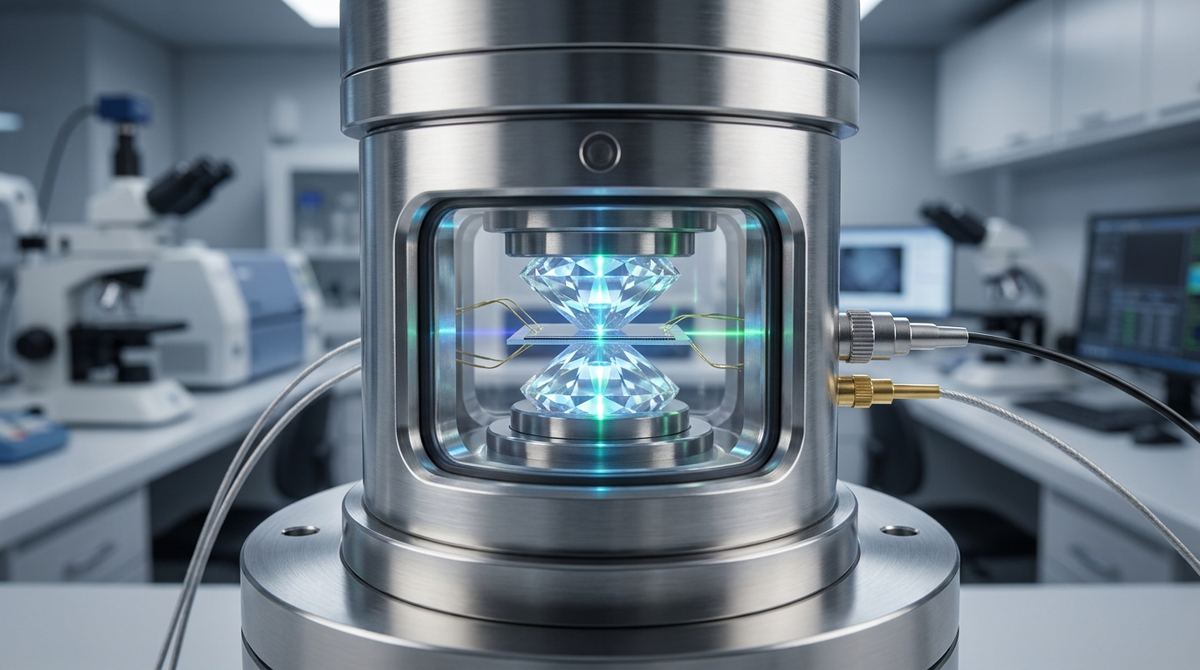
Engineers are constantly searching for pressure sensors that are smaller, more sensitive, and more stable. While MEMS and piezoresistive sensors dominate the market, they face limitations at the nanoscale and can be susceptible to drift and environmental interference. A recent breakthrough in materials science offers a completely new physical principle for pressure detection, one that leverages the strange quantum-mechanical behavior of 2D materials.
Research published in late 2026 by Lujin Min and a team of collaborators reveals an anomalous property in a material called a "sliding ferroelectric." Unlike conventional materials, where applying pressure crushes their special electrical properties, this new class of material actually gets stronger. Specifically, they found that the ferroelectric polarization of parallel-stacked bilayer boron nitride (BN) increases significantly and linearly under hydrostatic pressure.
This guide translates that fundamental discovery into a practical engineering project. We will outline the steps to build a prototype high-sensitivity pressure sensor. The device uses a single layer of graphene as an atomically thin detector to read the pressure-induced changes in the underlying bilayer BN. This project explores the frontier of slidetronics and offers a tangible way to experiment with some of the most advanced concepts in materials engineering. The potential applications for such a device are vast, from industrial process monitoring in harsh environments to novel scientific instrumentation.
The objective is to construct and test a device that transduces hydrostatic pressure into a measurable electrical signal. The core of the device is a van der Waals heterostructure, a carefully assembled stack of 2D materials.
The final device will be a field-effect transistor (FET) where:
1. The channel is made from a monolayer of graphene.
2. The graphene channel rests directly on a ferroelectric bilayer of hexagonal boron nitride (h-BN).
3. The h-BN and graphene stack is placed on a standard silicon dioxide/silicon (SiO2/Si) wafer, where the doped silicon acts as a back gate.
4. Metal contacts are patterned onto the graphene to measure its electrical properties.
The sensor's operation relies on the graphene's extreme sensitivity to its local electrical environment. The underlying ferroelectric BN creates an electric field that "dopes" the graphene, changing its conductivity. As pressure is applied, the BN's ferroelectric field gets stronger, which in turn changes the graphene's electrical properties in a predictable way. By measuring the graphene's resistance or its charge neutrality point (Dirac point), we can precisely determine the applied pressure.
To understand how this sensor works, we need to compare two types of ferroelectric materials.
In conventional ferroelectrics like barium titanate, the electrical polarization comes from a slight displacement of ions within the material's crystal lattice. Imagine a cage of atoms with one atom slightly off-center, creating a small electric dipole. When you apply hydrostatic pressure, you squeeze this crystal lattice, forcing the off-center atom back towards the middle. This weakens or completely suppresses the ferroelectric polarization.
Sliding ferroelectrics, a recently discovered class of materials, work differently. Here, the polarization arises not from atoms being displaced within a single layer, but from the precise way two or more layers are stacked on top of each other. In the case of bilayer h-BN, a slight lateral shift between the top and bottom layers creates a net charge transfer, resulting in an out-of-plane electric dipole. The polarization direction can be flipped by sliding one layer relative to the other.
The key finding from the source research is that applying hydrostatic pressure pushes the BN layers closer together. This vertical compression enhances the interlayer electronic interactions, which in turn boosts the charge transfer for a given lateral stacking. The result is a stronger ferroelectric polarization. The researchers observed an 80% linear increase in polarization as pressure was increased to 1.66 GPa. This counterintuitive, pressure-enhancing effect is the foundation of our sensor design. Graphene's role in next-generation electronics is often tied to its ability to interface with and detect subtle phenomena in such novel materials.
This is an advanced project that requires access to a cleanroom or a well-equipped materials science lab.
Materials:
Graphene: Monolayer CVD graphene on copper foil is the most practical starting point.
Hexagonal Boron Nitride (h-BN): High-quality h-BN crystals for mechanical exfoliation. You will be searching for bilayer flakes.
Substrate: Silicon wafers with a 285 nm or 300 nm thermal oxide layer (SiO2/Si). The oxide thickness is chosen to provide good optical contrast for 2D materials.
Transfer Polymers: Polymethyl methacrylate (PMMA) and a viscoelastic stamp material like polydimethylsiloxane (PDMS).
Solvents: Acetone, isopropyl alcohol (IPA), and removers for lithography resists.
Metal for Contacts: Chromium (5 nm adhesion layer) and Gold (50-100 nm conducting layer).
Process Gases: Argon and hydrogen for annealing.
Equipment:
Dry Transfer Station: A setup with high-precision micromanipulators and an optical microscope for stacking the 2D materials.
Optical Microscope: A high-quality reflected light microscope with magnification up to 100x for identifying 2D flakes.
Mechanical Exfoliation Tools: High-quality dicing tape or adhesive tape for exfoliating h-BN.
Lithography System: Electron-beam lithography is ideal for precise, small-scale contacts. A high-resolution photolithography setup can also work for initial prototypes.
Metal Deposition System: An e-beam evaporator or thermal evaporator for depositing the Cr/Au contacts.
Tube Furnace: For annealing the final device in a controlled atmosphere to clean the interfaces.
Probe Station and Semiconductor Analyzer: To perform electrical measurements (e.g., measuring resistance vs. gate voltage).
Hydrostatic Pressure Cell: This is the most specialized piece of equipment. A diamond anvil cell (DAC) is the gold standard. For initial tests, a piston-cylinder hydrostatic pressure apparatus may be more accessible, though it will likely have a lower pressure range. Access to such equipment may require collaboration with a university or specialized research lab.
Fabricating a high-quality van der Waals heterostructure is an art that requires patience and practice. Each step is critical to the final device performance.
1. Substrate Preparation:
Cleave a SiO2/Si wafer into appropriately sized chips (e.g., 1cm x 1cm).
Clean the chips thoroughly using a sequence of solvents: sonicate in acetone for 5 minutes, then IPA for 5 minutes.
Dry the chips with a nitrogen gun.
Perform an oxygen plasma ash or piranha clean if available to ensure a pristine, hydrophilic surface.
2. h-BN Exfoliation and Identification:
Press a piece of adhesive tape firmly onto a high-quality h-BN crystal.
Peel the tape off, bringing thin layers of h-BN with it.
Repeatedly fold and unfold the tape onto itself to further thin the flakes.
Gently press the tape onto your cleaned SiO2/Si substrate and then slowly peel it away, leaving behind exfoliated flakes.
Using an optical microscope, search for very thin flakes. Bilayer h-BN has a very faint optical contrast. You are looking for uniform, atomically flat regions. Confirmation often requires AFM or Raman spectroscopy, but for a prototype, you can proceed with promising candidates identified by optical contrast alone.
3. Heterostructure Assembly (Dry Transfer):
This process uses a polymer stamp (e.g., PDMS) to pick up and stack layers.
First, prepare the graphene. Spin-coat a layer of PMMA onto your CVD graphene/copper foil. Etch away the copper using a suitable etchant (e.g., ammonium persulfate). You are left with a PMMA/graphene film floating in water.
Pick up the PMMA/graphene film with your PDMS stamp.
Using the micromanipulators on your transfer station, carefully align the graphene over your target bilayer h-BN flake on the substrate.
Slowly lower the stamp until the graphene makes contact. Then, slowly heat the stage (around 100-150°C, this is an engineering assumption as the source does not specify) to release the PMMA/graphene stack onto the h-BN.
Dissolve the PMMA in an acetone bath, followed by an IPA rinse, leaving the graphene/h-BN stack on the substrate.
4. Device Fabrication:
Use your lithography system to pattern the desired geometry for the electrical contacts. A Hall bar geometry is ideal as it allows for more detailed characterization, but a simple two- or four-probe setup across the graphene flake is sufficient for a first prototype.
Deposit the Cr/Au metal contacts using your evaporator.
Perform liftoff by dissolving the remaining resist in a solvent bath, leaving only the metal contacts in the patterned areas.
5. Annealing:
Place the finished device in a tube furnace.
Anneal the device at 300-400°C under a flow of Ar/H2 gas for several hours. This critical step removes polymer residues and water trapped at the interfaces, ensuring the graphene is sensitive to the BN's electric field.
The goal is to measure the shift in graphene's Dirac point as a function of pressure.
1. Ambient Pressure Characterization:
Place your device on the probe station.
Connect the source and drain contacts to a source-measure unit and the silicon back gate to a voltage source.
Measure the graphene's resistance while sweeping the back-gate voltage (e.g., from -60V to +60V).
Plot the resistance vs. gate voltage. The peak of this curve is the Dirac point, which corresponds to the gate voltage needed to achieve charge neutrality in the graphene. Record this value.
2. Applying Hydrostatic Pressure:
Carefully mount your device inside the pressure cell. This process is highly specific to the equipment you are using.
Ensure the electrical connections are sound.
Use the pressure-transmitting medium specified for your cell (e.g., a silicone oil or a Daphne oil).
Slowly increase the pressure to your first setpoint, for example, 0.2 GPa. The source paper goes up to 1.66 GPa, but your initial range should be dictated by the limits of your equipment.
3. Data Collection Under Pressure:
At each pressure setpoint, repeat the gate voltage sweep and record the resistance vs. gate voltage curve.
Find the new position of the Dirac point. The ferroelectric polarization of the BN will induce charge carriers (doping) in the graphene. This doping shifts the Dirac point. An increase in polarization should cause a larger shift.
Repeat this measurement at several pressure increments (e.g., 0.2, 0.4, 0.6... GPa).
4. Data Analysis:
Create a plot of the Dirac point voltage shift (ΔV_Dirac) versus applied pressure (P).
Based on the source paper, you should expect a roughly linear relationship. The slope of this line is the sensitivity of your sensor (in Volts per GPa).
This plot serves as the calibration curve for your prototype pressure sensor. The results can inform future novel graphene sensor designs.
This project is challenging and relies on several assumptions.
Assumptions:
The most significant assumption is access to a hydrostatic pressure cell capable of reaching the GPa range while allowing for electrical measurements. These are not common pieces of equipment.
We assume that bilayer h-BN can be reliably identified using optical microscopy. In reality, this is difficult, and misidentification (e.g., using monolayer or trilayer) will lead to different or non-existent results.
The quality of the interfaces is assumed to be high after annealing. Any trapped residue can screen the ferroelectric field, muting or eliminating the sensor's response.
We assume the linear response observed in the research paper will hold for a prototype device that may have more defects and impurities.
Risks:
Device Failure: The heterostructure is fragile. The sheer stress and pressure during testing can cause the layers to delaminate, the substrate to crack, or the contacts to fail.
Fabrication Challenges: Creating clean, high-quality van der Waals heterostructures is notoriously difficult. Yields can be low, and it may take many attempts to produce a working device.
Measurement Noise: Electrical noise, temperature fluctuations, and gate leakage can obscure the relatively small signal you are trying to measure. Careful shielding and high-quality electronics are essential.
Material Sourcing: Acquiring high-quality h-BN crystals and monolayer CVD graphene is crucial. Lower-quality materials, such as some forms of bulk graphene powder, are not suitable for this application.
This engineering guide is directly inspired by the 2026 paper "Anomalous Pressure-Enhanced Polarization in Sliding Ferroelectrics" by Min et al. The core physical principle—that hydrostatic pressure enhances the polarization of bilayer h-BN—is taken directly from their experimental findings. Their use of a graphene layer to sense the polarization is adapted here to form the basis of the sensor itself.
While the paper establishes the science, this guide provides the engineering framework to build upon it. A successful prototype would be a significant achievement, demonstrating a new sensing modality. The next steps would involve optimizing the device design for higher sensitivity, exploring encapsulation techniques to protect the device, and integrating it into a more compact, user-friendly package. Investigating the commercial viability and market trends for such a high-performance sensor would be a logical follow-on activity for any startup or lab pursuing this technology. This work represents a small but exciting step toward a future of slidetronic devices.
For related commercial context, explore turbostratic graphene flakes and graphene production machinery.
Serious about B2B integration? Test our premium Pulsed Electrical Resistive Carbon Heating turbostratic graphene in your lab. 100g sample packs available now.
Explore More
Explore how the intrinsic band geometry of 2D materials can induce valley polarization of chiral excitons, a key step toward next-gen valleytronics.

Researchers predict a new physical effect in gapless Dirac materials like graphene, where propagating waves can induce a direct DC current without a p-n...

Explore how the superfluid weight in magic-angle graphene is driven by quantum geometry, a discovery that could redefine our search for new superconductors.