
Practical Guide: Prototyping a Graphene Superlattice Quantum Sensor
Explore how a gate-defined graphene superlattice can create a versatile quantum sensor, leveraging unique electron states for advanced magnetic field detection.
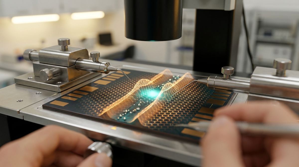
At the heart of every technological leap, from the first transistor to the most advanced quantum computer, lies a single, fundamental challenge: control. Specifically, the ability to precisely control the behavior of electrons within a material. For decades, engineers have relied on silicon to build ever-smaller and more powerful devices. But as we approach the physical limits of silicon, a new frontier is emerging in materials like graphene, where the rules of physics offer both greater challenges and more profound opportunities. A recent theoretical paper provides a fascinating new mathematical roadmap for navigating this frontier, offering a blueprint for controlling electrons in ways previously unimaginable. This research, while deeply rooted in the abstract world of high-energy physics, provides a powerful analogy for designing the next generation of graphene-based electronics.
To build a better switch, sensor, or processor, engineers need to create and manage tiny, well-defined pathways for electrons. In traditional electronics, this is done by doping silicon, creating junctions between different material types. In the world of 2D materials like graphene, a more elegant approach is possible: engineering the very structure of the material itself to create "virtual" channels. This could involve creating folds, wrinkles, or boundaries between regions with different properties. The problem is that a robust, predictive theory for how electrons behave when trapped between two such engineered boundaries has been elusive. Engineers often rely on a degree of trial and error. How does the electron's energy change as the boundaries get closer? How tightly can we confine the electron? What happens at the exact moment the two boundaries merge into one? Without a clear mathematical framework to answer these questions, designing novel nanoelectronic devices remains an inefficient, intuition-driven process. The work by physicists H. P. Pinheiro and C. A. S. Almeida addresses this gap by providing a precise analytical model for just such a scenario.
Imagine a vast, flat plain representing a sheet of graphene. On this plain, electrons can roam freely. Now, imagine creating two parallel "fences" or energy walls on this plain. These fences are not physical barriers but are instead generated by subtle changes in the underlying properties of the graphene sheet. In the language of theoretical physics, these fences are called "kinks" or "domain walls." The core idea of this research is to mathematically describe what happens to an electron—a type of particle known as a fermion—that gets trapped in the channel between these two fences. The paper develops a model that allows physicists to predict the electron's properties, such as its energy level and where it's most likely to be found, based on a single, crucial parameter: the distance between the two fences. It provides a formula for "tuning" the electron's state simply by adjusting the spacing of these engineered boundaries. Most profoundly, it predicts a strange and powerful behavior when the two fences are pushed together until they merge, a phenomenon the authors call a "universal divergence."
While the original paper is formulated in the abstract language of high-energy field theory, its principles can be translated into a tangible system using graphene. In this analogy, the "two-kink scalar background" described by the theory is not some exotic feature of spacetime, but rather an engineered landscape on a graphene sheet. The two "kinks" can be thought of as two parallel line defects, folds, or grain boundaries. These could be created using advanced fabrication techniques that modify the structure or electronic properties of the graphene along a precise line. For example, one could use a focused ion beam to subtly damage the lattice or apply strain with a patterned substrate to create these energy walls. The electrons flowing within the graphene then take on the role of the "chiral fermions" from the model. Graphene is an ideal material for this because its electrons behave in a unique way, mimicking the massless, relativistic particles of high-energy physics, a property that makes them particularly sensitive to these kinds of structural boundaries. The "tunable brane positioning" from the paper's title translates directly to the engineer's ability to control the distance between these two line defects. By applying an electric field or mechanical stress, it might be possible to dynamically change this separation, thereby tuning the properties of the electronic channel between them, as described by the model. This system transforms defects from unwanted imperfections into precision tools for electronic design, a central goal in the field of graphene electronics.
Pinheiro and Almeida's work produced a clear and elegant mathematical solution describing the behavior of a fermion trapped between two kinks. Their first key finding is that a stable, localized state for the fermion exists, and its properties are directly and continuously dependent on the distance separating the two kinks. This confirms that such a system can be used as a tunable electronic component; change the distance, and you predictably change the electron's energy and quantum state. The second, and more striking, discovery relates to the "single-kink limit." They calculated what happens as the distance between the two kinks approaches zero. At this limit, where the two boundaries merge, they found that a key physical quantity associated with the fermion's localization diverges, meaning it shoots towards infinity. Critically, they showed this divergence is "universal." This means the mathematical form of this blow-up is the same regardless of the specific shape or profile of the kinks. This universality is incredibly powerful. It implies that engineers don't need to create perfectly identical or shaped defects to observe this extreme effect; as long as they can bring two boundary-like features together, this predictable phenomenon should emerge. It provides a robust design target that is less sensitive to manufacturing imperfections.
This theoretical result, though abstract, is significant because it provides a new set of design rules for nano-scale engineering. The concept of tunable localization offers a pathway to creating new kinds of electronic switches. Instead of using a traditional gate voltage to allow or block current, a device could function by mechanically or electrically adjusting the distance between two line defects, effectively opening or closing a conductive channel. The discovery of the universal divergence is even more profound. In science and engineering, divergences are not typically errors but signals of new and interesting physics. This predictable, infinite response at the single-kink limit suggests that the point where two engineered boundaries meet is a "hot spot" of extreme electronic activity. A device designed to operate near this limit could exhibit unprecedented sensitivity. It shifts the paradigm from viewing material interfaces as passive boundaries to seeing them as active, tunable components whose interactions can be harnessed for novel functions. This model-driven approach could accelerate the development of complex devices, reducing the reliance on costly and time-consuming experimental iteration, a key factor in improving the scalability of graphene manufacturing techniques.
It is crucial to understand the context and limitations of this work. This is a theoretical paper in the domain of mathematical physics. The model is a simplified one, existing in one spatial dimension plus time (1+1 dimensions). A real graphene sheet is two-dimensional, and the electrons move within that plane. The model also does not account for real-world complexities such as temperature effects, material impurities, electron-electron interactions, or the influence of the substrate the graphene rests on. These factors could potentially alter or mask the predicted behaviors. Therefore, the most important next step is experimental validation. Materials scientists and physicists now have a clear theoretical prediction to test. The challenge is to fabricate a system in graphene or a similar 2D material with two controllable, closely-spaced line defects and then to use techniques like scanning tunneling microscopy to measure the electronic states in the channel between them. The ultimate test will be to see if the predicted universal divergence can be observed as these defects are made to merge.
Should the predictions of this model be experimentally verified, they could unlock a range of next-generation technologies built on the principle of defect engineering. One of the most immediate applications would be in the realm of ultra-sensitive sensors. A device built around two nearly-merged kinks could act as an exceptional strain sensor; even a minuscule change in the material's physical dimensions would drastically alter the distance between the kinks, producing a massive and easily detectable electronic signal. This principle could be applied to create advanced graphene sensors for detecting pressure, vibrations, or specific chemical bindings. In electronics, this could form the basis of a new type of transistor, a "topological" switch, where the on/off state is controlled by the merging and separation of these engineered channels. Furthermore, the ability to create and precisely tune a localized quantum state for an electron is a foundational requirement for quantum computing. This model provides a potential new method for creating and manipulating qubits, the building blocks of quantum information, by controlling the geometry of the material itself.
If there is one central lesson to take from this research, it is this: the engineered interfaces and defects within a material like graphene are not just passive boundaries, but active and powerful design elements. The space between two such defects forms a tunable electronic component whose properties can be controlled with geometric precision. And the point where these defects merge is not a flaw, but a source of predictable and extreme physical behavior that can be harnessed for new technologies.
What is a chiral fermion in the context of graphene?
In high-energy physics, chirality refers to the "handedness" of a particle. In the context of graphene, electrons behave in a special way that allows them to be described by the same mathematics used for massless chiral fermions. This means an electron's direction of motion is locked to another of its quantum properties, called pseudospin. This unique behavior is what makes electrons in graphene so sensitive to the kinds of engineered structural boundaries discussed in this research.
What does a "kink" or "domain wall" represent in a real material?
In the abstract theory, a kink is a stable, localized transition between two different vacuum states of a field. In a real material like graphene, this translates to a physical boundary or interface. It could be a fold in the graphene sheet, a boundary between two crystal domains that are oriented differently, or a line where the graphene has been chemically modified or sits on a different substrate, creating a sharp change in its electronic potential.
Is this research about cosmology or materials science?
This research is fundamentally a work of theoretical high-energy physics ("hep-th"), which often explores concepts like braneworlds from string theory, where our universe is a "brane" in a higher-dimensional space. However, the mathematical framework developed is general enough to be applied to other systems. The connection to materials science and graphene is a powerful analogy, where the 2D graphene sheet acts like the "brane" and the electrons within it behave like the "chiral fermions" of the model.
Why would a "divergence," which sounds like a mathematical error, be useful?
In physics, a divergence or infinity in a model often signals that the model is being pushed to its limit, revealing a point of critical behavior. Rather than an error, it's a feature. A system that exhibits a divergent response to a small input is, by definition, infinitely sensitive. Engineers can design devices to operate near, but not exactly at, this point of divergence to create sensors or switches with an enormous and predictable response.
How long until we see devices based on this principle?
This research is at the earliest, most fundamental stage. It provides a theoretical target for experimentalists to pursue. The next steps involve years of work in materials science labs to first create and control such "two-kink" systems in graphene and then to verify that the electrons behave as predicted. If these experiments are successful, it would likely take another decade or more of engineering development to translate these principles into commercially viable devices.
The research by H. P. Pinheiro and C. A. S. Almeida provides a beautiful example of how the most abstract explorations in theoretical physics can offer profound insights for practical engineering. By developing an exact model for fermion localization in a two-kink system, they have provided a new language and a predictive framework for the field of nanoelectronics. Their work suggests that the future of electronics may not lie in simply shrinking old designs, but in embracing a new paradigm where the very fabric of a material is engineered with geometric precision. By treating defects and interfaces as tunable components, this research illuminates a path toward creating devices whose performance is limited only by the laws of physics themselves.
Serious about B2B integration? Test our premium Pulsed Electrical Resistive Carbon Heating turbostratic graphene in your lab. 100g sample packs available now.
Explore More
Explore how a gate-defined graphene superlattice can create a versatile quantum sensor, leveraging unique electron states for advanced magnetic field detection.

New research introduces a controlled loop expansion for the topological heavy fermion model, a powerful theoretical tool for designing future quantum materials.

Researchers derived an analytic formula for twisted bilayer graphene electron lifetimes, providing a key design tool for future quantum and electronic devices.