
Chiral Fermion Localization: A New Blueprint for Graphene Nanoelectronics
Explore chiral fermion localization in two-kink systems. This theoretical physics research offers a powerful new model for controlling electrons in...
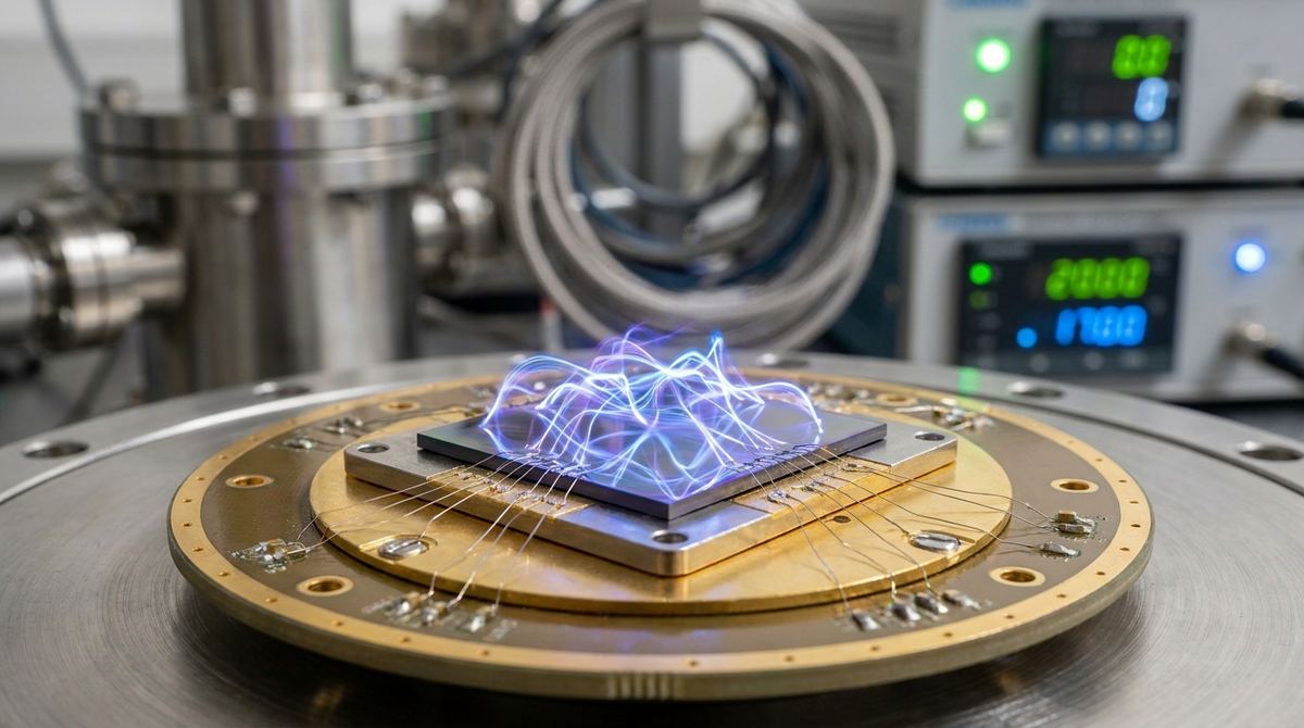
Graphene's unique electronic properties have made it a cornerstone material for next-generation electronics. One of the most powerful techniques for harnessing its potential is the creation of artificial superlattices. A superlattice is a periodic structure of alternating materials, but in graphene, we can create one without any chemical modification. By placing a series of nanoscale gates beneath or on top of a graphene sheet, we can impose a periodic electrostatic potential, effectively tricking electrons into behaving as if they are in a different material. This gate-defined approach offers unparalleled tunability, allowing us to engineer the electronic band structure of graphene on the fly.
A recent study by Che-Pin Hsu and colleagues (2026) explores a particularly elegant device architecture: a normal graphene (NGr) region, followed by a superlattice graphene (SGr) region, and another normal graphene region (NGr-SGr-NGr). This junction, all created on a single, continuous sheet of graphene, acts as a versatile platform for observing a rich variety of quantum transport phenomena. Depending on the applied gate voltages and magnetic field, the device can operate in distinct regimes, exhibiting everything from classic wave interference to exotic electron trajectories.
This guide translates the fundamental research of Hsu et al. into a practical plan for engineers and small labs. We will outline the steps to design, fabricate, and test a prototype multi-mode quantum sensor based on the NGr-SGr-NGr junction. This single device can function as a highly sensitive magnetometer or a research tool for exploring quantum physics, showcasing the immense potential of engineered graphene applications.
To build this device, we first need to understand the underlying physics. The core of the prototype is the NGr-SGr-NGr junction. Imagine a perfectly flat, single-lane highway representing your sheet of graphene. The NGr regions are the normal, unobstructed parts of the highway. The SGr region is a section where a series of precisely spaced, invisible speed bumps have been installed. These "speed bumps" are not physical; they are areas of higher or lower electric potential created by the array of gates.
When electrons travel through the SGr region, this periodic potential fundamentally changes their behavior. The paper highlights that it renormalizes their Fermi velocity, meaning it effectively changes the speed at which they carry energy. This difference in electron velocity between the NGr and SGr regions is the key to the device's function. The interface between these regions acts like a boundary between two different optical media, causing electron waves to reflect and refract in interesting ways.
The device's behavior is further controlled by an external magnetic field applied perpendicular to the graphene sheet. A magnetic field forces moving electrons to travel in curved paths, known as cyclotron orbits. The interplay between the superlattice potential and the magnetic field gives rise to the three distinct operational modes of our sensor:
1. Low-Field Regime (Fabry-Pérot Interference): At very low magnetic fields, the SGr region acts as a resonant cavity for electron waves. Waves bounce back and forth between the two NGr-SGr interfaces, creating interference patterns. The device's conductance will oscillate as you change the carrier density (via a back gate), a phenomenon known as Fabry-Pérot interference.
2. Intermediate-Field Regime (Supersnake States): This is where the most novel physics occurs. At intermediate magnetic fields, electrons attempting to cross the NGr-SGr boundary are forced into a unique trajectory. They travel in a conventional semicircular arc on the NGr side and then an anomalous, differently curved arc on the SGr side. The result is a weaving, snake-like path that propagates along the junction boundary. These "supersnake states" are stable transport channels that produce their own characteristic oscillations in the device's conductance, highly sensitive to the magnetic field strength.
3. High-Field Regime (Hofstadter Butterfly): At stronger magnetic fields (up to 3 Tesla in the source paper), the system's energy levels split into a complex, fractal pattern known as the Hofstadter butterfly. A plot of conductance versus magnetic field and carrier density will reveal this iconic quantum mechanical spectrum.
Our goal is to build a single device that can be tuned to operate in any of these three regimes, creating a uniquely versatile quantum sensor.
Fabricating a quantum device requires a cleanroom environment and specialized equipment. Here is a list of what you will need to get started.
Materials:
Substrate: Standard silicon wafers with a 285 nm or 300 nm thermal oxide layer (Si/SiO2). The heavily doped silicon serves as a global back gate.
Graphene: High-quality, single-layer graphene is essential. For initial prototypes, mechanically exfoliated flakes from kish graphite or highly ordered pyrolytic graphite (HOPG) offer the highest electronic quality. For more scalable production, high-quality CVD-grown graphene on copper, which is then transferred to the Si/SiO2 substrate, is the preferred method. For bulk processing experiments, materials like turbostratic graphene flakes could be explored for different device types, though monolayer quality is key here.
Dielectric Layer: A high-quality, ultra-thin insulating layer is needed to separate the top gates from the graphene. Hexagonal boron nitride (h-BN) is the ideal choice due to its atomically flat surface and low defect density. Alternatively, a thin layer (5-10 nm) of aluminum oxide (Al2O3) or hafnium oxide (HfO2) deposited via Atomic Layer Deposition (ALD) is a viable option.
Metals: Chrome (Cr) or Titanium (Ti) as an adhesion layer (5 nm) and Gold (Au) as the contact metal (50-100 nm) for source, drain, and gate electrodes.
Equipment:
Fabrication: An electron-beam lithography (EBL) system for high-resolution patterning of contacts and nanoscale gates. A photolithography setup can be used for larger features like contact pads.
Deposition: A metal evaporator (thermal or e-beam) for depositing the contact and gate metals. An ALD system if you are using oxide dielectrics.
Etching: A reactive-ion etching (RIE) system with oxygen plasma for shaping the graphene into the desired device geometry (e.g., a Hall bar).
Measurement: A probe station for initial room-temperature tests. For low-temperature measurements, a cryostat (e.g., a Physical Property Measurement System or a simple liquid helium dipstick probe) is required.
Electronics: A set of low-noise DC voltage sources for the gates. For conductance measurements, a lock-in amplifier paired with a low-frequency AC voltage source and a current preamplifier is the standard, providing excellent signal-to-noise.
Magnetic Field: A superconducting magnet capable of reaching fields of at least 3-5 Tesla.
The following is a proposed fabrication flow. The exact parameters will need optimization based on your specific equipment and materials.
1. Substrate Preparation: Begin with a clean Si/SiO2 wafer. Use a standard cleaning procedure (e.g., piranha etch or RCA clean) to ensure a pristine surface.
2. Graphene Transfer: If using CVD graphene, transfer the monolayer sheet onto the SiO2 surface. If using exfoliated graphene, identify suitable single-layer flakes using optical microscopy and Raman spectroscopy.
3. Source and Drain Contact Definition: Use EBL to pattern the source and drain contacts. Develop the resist and then deposit Cr/Au (e.g., 5 nm / 50 nm) using an e-beam evaporator. Use a lift-off process in acetone to remove the excess metal, leaving only the contacts.
4. Graphene Channel Definition: Protect the channel area and contacts with EBL resist. Use a gentle oxygen plasma RIE to etch away the unwanted graphene, defining the device mesa (typically a Hall bar shape with a width of 1-5 micrometers).
5. Top Gate Dielectric Deposition: This is a critical step. If using h-BN, you will need to exfoliate a thin flake and transfer it precisely over the graphene channel using a dry-transfer technique. If using an oxide, deposit a thin, uniform layer of Al2O3 or HfO2 (e.g., 10 nm) over the entire device using ALD.
6. Superlattice Gate Patterning: Use EBL again to define the pattern for the periodic finger gates over the central region of the graphene channel. The source paper does not specify dimensions, so we will propose a starting point based on common practice.
Engineering Assumption: Let's target a superlattice period (L) of 80 nm, with a 50% duty cycle (40 nm wide gate, 40 nm gap). The total length of the SGr region could be around 1-2 micrometers.
7. Gate Metal Deposition: After developing the EBL resist, deposit the gate metal (e.g., 5 nm Ti / 40 nm Au). Perform lift-off to finalize the gate structure. You will need to pattern larger pads connecting to these gates for wire bonding.
8. Annealing and Packaging: Perform a final annealing step in a forming gas (Ar/H2) environment at around 300-400°C. This helps clean the graphene surface and improve contact resistance. Mount the chip onto a chip carrier and use a wire bonder to connect the device pads to the carrier pins.
Your goal is to systematically probe the three transport regimes identified in the source research. All measurements should be performed at low temperatures.
Assumption: The paper implies quantum coherence is necessary, so a starting temperature of 4.2 K (liquid helium) is a reasonable assumption.
1. Initial Device Check: Before cooling down, perform a simple two-terminal resistance measurement. Then, at 4.2 K, measure the channel resistance while sweeping the back-gate voltage. This will produce a resistance peak at the Dirac point (charge neutrality point) and confirm your device is functional and of good quality.
2. Mapping the Fabry-Pérot Regime:
Set the magnetic field to zero or a very low value (B < 0.1 T).
Apply a modulating voltage to the superlattice gates. For example, apply Vg1 to one set of fingers and Vg2 to the interdigitated set to create a periodic potential. A typical starting voltage might be +/- 1V.
Measure the two-terminal conductance (G) as you sweep the back-gate voltage (Vbg).
You should observe rapid oscillations in conductance superimposed on the background Vbg sweep. These are the Fabry-Pérot fringes. Analyze their frequency and amplitude as a function of the superlattice gate voltage.
3. Observing Supersnake States:
Increase the magnetic field to the intermediate regime (e.g., B = 0.5 T to 1.5 T).
Perform a 2D sweep. Measure conductance (G) while sweeping both the magnetic field (B) and the back-gate voltage (Vbg).
Plot the results as a color map of G(B, Vbg). Look for distinct, sharp lines or oscillations that do not correspond to standard Shubnikov-de Haas oscillations. These are the signatures of the supersnake states. According to the paper, their position should agree with semiclassical calculations based on your device geometry.
4. Revealing the Hofstadter Butterfly:
Sweep the magnetic field to higher values (B = 1 T to 3 T or more).
Perform another high-resolution 2D map of conductance G(B, Vbg).
Plot the data, possibly as its derivative (dG/dVbg), to enhance the features. You are looking for the characteristic self-similar, fractal pattern of the Hofstadter spectrum. This is a challenging but definitive confirmation of a high-quality superlattice.
Building this device is a significant undertaking with several challenges.
Fabrication Precision: The quality of the superlattice is paramount. The nanoscale gates must be uniform and well-defined. Any disorder can wash out the quantum effects. This requires state-of-the-art EBL and cleanroom practices. Access to such graphene production machinery is often the biggest barrier for small labs.
Graphene Quality: The electron mean free path in your graphene must be longer than the device dimensions. Any defects, impurities, or residue from the fabrication process will scatter electrons and destroy the quantum coherence needed to observe these effects.
Dielectric Integrity: The top gate dielectric must be pinhole-free. Any leakage from the gates to the graphene will render the device unusable. This is why h-BN is preferred, though ALD oxides can work if deposited with care.
Measurement Sensitivity: The conductance oscillations can be subtle. A low-noise measurement setup, including proper filtering and grounding, is essential. Using a lock-in technique at a low frequency (e.g., 17.77 Hz) is standard practice.
While this prototype is a research instrument, the underlying principles have commercial potential. The extreme sensitivity of the supersnake states to the magnetic field and carrier density could form the basis for a new class of Hall-effect sensors or magnetometers with unique operating principles. The ability to switch between distinct physical regimes on a single chip could be valuable for reconfigurable graphene electronics. For example, the same device could act as a filter in the Fabry-Pérot regime and a magnetic switch in the supersnake regime.
Furthermore, as the authors of the source paper note, this concept is not limited to graphene. It can be generalized to other 2D materials, opening up a wide field for materials engineering. As fabrication techniques improve and the costs associated with them decrease, we may see these quantum-engineered devices move from the lab into specialized commercial applications. Analyzing graphene market research can help identify niche areas, such as scientific instrumentation or quantum computing hardware, where such advanced sensors could find an early market.
This practical guide is based on the concepts and results presented in the 2026 preprint "Quantum transport across normal-superlattice-normal graphene junctions" by Hsu et al. The core ideas of the NGr-SGr-NGr junction, Fabry-Pérot interference, the Hofstadter butterfly spectrum, and the novel supersnake states are taken directly from this work.
The following specific parameters are engineering assumptions made for the purpose of creating a practical guide, as they were not detailed in the source abstract:
Device Dimensions: Channel width of 1-5 µm, superlattice period of 80 nm, and SGr region length of 1-2 µm.
Fabrication Materials: Specific choice of Cr/Au for contacts, Al2O3 as an alternative to h-BN, and specific metal thicknesses.
Operating Conditions: Assumed operating temperature of 4.2 K. Specific voltage ranges for gates.
Process Flow: The detailed step-by-step fabrication process is a standard but assumed workflow for creating such a device.
These assumptions provide a concrete starting point for any team looking to explore this exciting area of graphene nanoelectronics.
Serious about B2B integration? Test our premium Pulsed Electrical Resistive Carbon Heating turbostratic graphene in your lab. 100g sample packs available now.
Explore More
Explore chiral fermion localization in two-kink systems. This theoretical physics research offers a powerful new model for controlling electrons in...

New research introduces a controlled loop expansion for the topological heavy fermion model, a powerful theoretical tool for designing future quantum materials.

Researchers derived an analytic formula for twisted bilayer graphene electron lifetimes, providing a key design tool for future quantum and electronic devices.