
Interaction-driven transport in a non-degenerate mixture of Dirac and massive
Researchers explore interaction-driven transport in graphene, where massless Dirac fermions can drag massive particles, creating a current without direct...
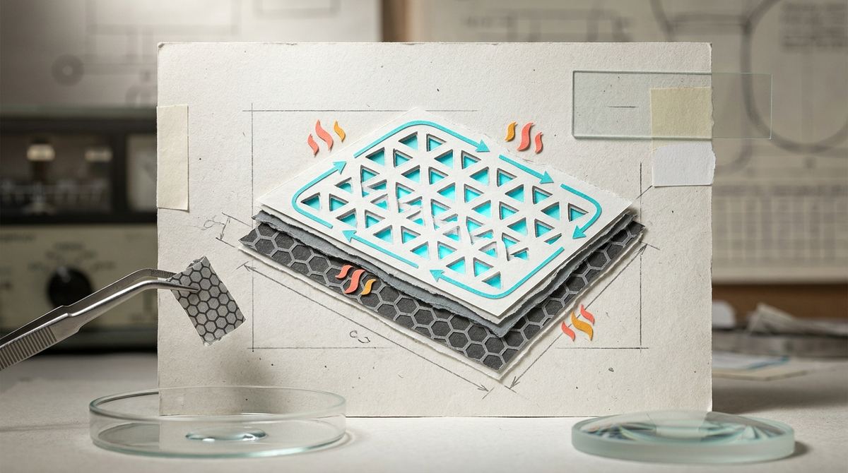
Imagine a highway system where traffic never slows down, regardless of how many potholes, bumps, or construction zones exist on the road. In the world of traditional electronics, electrons behave like cars on a bumpy road, constantly bumping into imperfections and losing energy as heat. This heat is the primary reason your smartphone gets warm and why supercomputers require massive cooling systems. Physicists are now looking for ways to create a highway where the cars are physically unable to turn around or crash, allowing them to flow perfectly along the edges of the road without ever losing speed. This concept, known as topological protection, could revolutionize how we build computers. Recent research into the structural manipulation of graphene suggests we are closer than ever to making this a reality.
The current era of semiconductor technology is facing a significant physical barrier known as the thermal wall. As we attempt to make electronic components smaller and faster, the density of transistors increases, leading to a massive concentration of heat. This heat is caused by the fundamental behavior of electrons moving through a material. In standard conductors like copper or silicon, electrons do not travel in a straight, perfect line. Instead, they undergo scattering.
Scattering occurs when an electron encounters a defect in the crystal lattice, a stray atom, or a vibration in the material structure. Every time an electron scatters, its kinetic energy is converted into thermal energy. This process, known as Ohmic heating, is the primary source of energy waste in modern computing. Because heat can damage delicate components and limits how much power can be pumped through a circuit, engineers are hitting a ceiling. We cannot simply keep shrinking transistors if the heat generated at that scale becomes unmanageable. To move past this, we need a way to move electrons that is fundamentally different from the way we move them today. We need materials where the electronic properties are protected by the very geometry of the material itself, ensuring that electrons can bypass obstacles without scattering.
To solve this, scientists are turning to a concept called topology. In mathematics, topology is the study of shapes and how they can be transformed. For example, a coffee mug and a donut are considered topologically identical because they both have exactly one hole. You could theoretically reshape a clay donut into a clay mug without ever tearing the material or sealing the hole. This "robustness" is the key. If a property of a material is topological, it means that small changes—like a few missing atoms or a slight dent in the surface—do not change the fundamental behavior of the electrons.
The researchers, Yong-Cheng Jiang, Xing-Xiang Wang, and Xiao Hu, are applying this mathematical concept to graphene. Graphene is a single layer of carbon atoms arranged in a hexagonal lattice. While graphene is an incredible conductor, its electrons follow certain rules that don't always allow for the specific type of topological protection we need for advanced computing. The idea is to introduce a new layer of "rules" by physically altering the graphene. By drilling a very specific, highly organized pattern of tiny holes into the graphene sheet, we create a new landscape for the electrons. This pattern, known as a superlattice, changes the way electrons perceive the material, potentially forcing them into these protected, unstoppable paths.
To understand how this works, we have to look at the relationship between a material's structure and its electronic band structure. In a pristine sheet of graphene, the electrons behave as if they have no mass. They move through the hexagonal lattice in a very specific way, governed by the symmetry of the carbon atoms. This creates what is known as a Dirac cone, a specific energy state that allows for high mobility. However, to achieve topological properties, we need to modify this energy landscape.
By introducing a triangular array of nanoholes, the researchers are creating a periodic potential. Imagine the original hexagonal lattice of graphene as a flat, smooth floor. When you add the triangular array of holes, you are essentially placing a series of rhythmic, geometric obstacles across that floor. These obstacles are not random; they are highly ordered. Because they are ordered, the electrons do not see them as random bumps that cause scattering. Instead, the electrons see them as a new, larger pattern.
This new pattern is called a superlattice. The interaction between the original carbon lattice and the new pattern of holes creates a new set of energy rules for the electrons. The triangular symmetry of the holes is crucial here. Symmetry is the language of physics. When you change the symmetry of a material by adding a pattern of holes, you change the electronic band structure. Specifically, this can create a "topological gap." This gap acts as a barrier that prevents electrons from scattering backward. Instead, the electrons are forced to move along the edges of the holes or the edges of the material. Because they are "topologically protected," they cannot be easily knocked off their path by a defect or an impurity. The geometry of the holes essentially creates a one-way street for electrons.
The research conducted by Yong-Cheng Jiang, Xing-Xiang Wang, and Xiao Hu focuses on how these specific triangular patterns influence the topological properties of the graphene sheet. Their work indicates that the introduction of a periodic array of nanoholes can successfully induce specific topological characteristics that were not present in the original, continuous sheet of graphene.
By carefully calculating the electronic properties, the study suggests that the triangular arrangement is particularly effective at creating the necessary symmetry-breaking required to produce these states. The findings imply that the nanoholes act as an artificial gauge field, which is a way of saying they manipulate the electron as if a magnetic field were present, even when no actual magnet is nearby. This manipulation results in the emergence of topological features in the electronic density of states. This means that the electrons are no longer just moving through a sheet; they are moving through a carefully engineered landscape designed to control their flow and protect them from the energy loss caused by scattering.
The implications of these findings are profound for the future of condensed matter physics and electronic engineering. If we can reliably create materials with topological protection, we can move from the era of classical electronics to the era of topological electronics. The primary benefit is the reduction of energy dissipation. As we discussed, the goal is to create circuits where electrons move without resistance-induced heating. If electrons can flow along protected paths without scattering, the amount of heat generated by a microchip would drop significantly.
Furthermore, this research provides a blueprint for "band engineering." Instead of searching for rare, naturally occurring topological materials in the earth's crust, we can use manufacturing techniques to "program" the properties of common materials like graphene. This ability to custom-design the behavior of electrons by simply changing the physical pattern of a material is a massive leap forward. It moves us from being observers of material properties to being architects of them. This could lead to a new generation of highly efficient, high-frequency devices that operate at speeds and power levels currently thought to be physically impossible.
While the theoretical and computational results are exciting, it is important to distinguish these findings from a commercially ready product. The research currently exists in the realm of fundamental physics and advanced modeling. One of the most significant challenges is the fabrication of these nanoholes. To achieve the topological effects predicted, the holes must be placed with near-perfect precision and uniformity across the entire sheet of graphene.
Current nanofabrication techniques, such as electron-beam lithography, are extremely precise but are also very slow and expensive. Scaling this process up to manufacture millions of chips for consumer electronics is a massive engineering hurdle. Additionally, the presence of even a single misplaced hole or a slight irregularity in the triangular pattern could disrupt the topological protection. Future research will need to focus on how these topological properties hold up in real-world conditions, where material imperfections are inevitable. We also need to determine how these patterns interact with other components in a functional electronic circuit to ensure the benefits are not lost when the material is integrated into a larger system.
The potential applications for graphene with nanohole arrays span several high-tech industries. In the realm of quantum computing, topological protection is a holy grail. One of the biggest problems in quantum computing is "decoherence," where the quantum state of a qubit is destroyed by environmental noise. If we can create topological electronic states, we might be able to create "topologically protected qubits" that are inherently resistant to noise, making quantum computers much more stable and scalable.
In the field of high-speed communications, these materials could be used to create ultra-fast transistors and oscillators. Because the electrons move with such high mobility and low heat, devices could operate at much higher frequencies than current silicon-based components. This would be critical for the development of 6G networks and advanced satellite communications. Finally, in the field of sensing, the sensitivity of the electronic states to the geometry of the holes could allow for the creation of incredibly precise sensors capable of detecting single molecules or minute changes in the environment.
If you remember only one thing from this research, let it be this: by using precise geometric patterns to alter the structure of graphene, scientists are learning how to "protect" the flow of electrons, potentially eliminating the heat and energy waste that currently limits the power of our computers.
Question: What is the main difference between graphene and graphene with nanoholes? Answer: Pristine graphene is a single layer of carbon atoms that conducts electricity very well but is subject to electron scattering, which causes heat. Graphene with a triangular array of nanoholes has a new, repeating pattern that changes how electrons behave, creating a superlattice that can protect electrons from scattering through topological properties.
Question: Why is "topology" such a big deal in physics? Answer: Topology is important because it deals with properties that are resistant to small changes or defects. In electronics, if a property is topological, it means the electron's path is "locked" by the geometry of the material, meaning it can't easily be knocked off course by a bump or an impurity, which reduces energy loss.
Question: Will this technology make my phone battery last longer? Answer: While this research is currently in the fundamental science stage and not ready for mass production, the ultimate goal is to create materials that generate much less heat. If successful, this could lead to much more energy-efficient electronics, which would directly translate to longer battery life for all portable devices.
Question: Why do the holes need to be in a triangular pattern? Answer: The pattern of the holes determines the symmetry of the material. The researchers found that a triangular array creates a specific type of symmetry that, when combined with graphene's hexagonal structure, produces the specific electronic band structures needed for topological protection.
Question: How do researchers actually make these tiny holes? Answer: Scientists use advanced nanofabrication tools such as electron-beam lithography or focused ion beam systems. These tools can move atoms or remove them with extreme precision, though they are currently much slower and more expensive than the processes used to make standard silicon chips.
The work by Jiang, Wang, and Hu represents a significant step in the ongoing quest to master the behavior of electrons at the atomic scale. By moving beyond the simple study of materials and toward the active "engineering" of their topological properties, we are opening a new frontier in condensed matter physics. While the path from a mathematical model of a triangular nanohole array to a mass-produced computer chip is filled with engineering challenges, the potential reward—a world of dissipationless, ultra-efficient, and incredibly fast electronics—is enough to drive the scientific community forward for decades to come.
Serious about B2B integration? Test our premium Pulsed Electrical Resistive Carbon Heating turbostratic graphene in your lab. 100g sample packs available now.
Explore More
Researchers explore interaction-driven transport in graphene, where massless Dirac fermions can drag massive particles, creating a current without direct...

Researchers have developed a high-efficiency graphene-silicon microring modulator, a critical step toward faster, lower-power optical communications and...

Build a near-infrared photodetector with nitrogen-doped porous graphene nanoribbons. This guide details the materials, fabrication steps, and test plan.