
3D Atomic Imaging of Graphene Dynamics from a Single Low-Dose TEM Snapshot
A new physics-informed AI method reconstructs the 3D atomic structure and dynamics of graphene from a single low-dose TEM image, solving a key imaging...
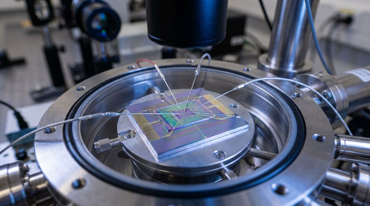
The field of spintronics has traditionally relied on the Jullière model, where magnetoresistance (MR) is a function of the spin polarization of the electrodes. However, recent research into van der Waals (vdW) heterostructures has revealed a more powerful mechanism: spin-dependent interlayer hybridization. By stacking graphene with the antiferromagnet CrSBr, engineers can create devices where the magnetic state of the CrSBr layer directly modifies the electronic band structure of the graphene. This results in massive, bias-tunable magnetoresistance that can reach up to 350 percent. For engineers developing next-generation magnetic sensors or non-volatile memory, this offers a pathway to extreme sensitivity that is controllable through external voltage.
The primary application for this technology is the development of ultra-sensitive magnetic field sensors operating at cryogenic temperatures. Unlike standard Hall effect sensors or traditional Giant Magnetoresistance (GMR) sensors, these heterostructures allow for a tuning knob via bias voltage. By applying a specific voltage, you can shift the device into a regime where the magnetoresistance is maximized, making the sensor incredibly responsive to minute changes in the magnetic field orientation. This makes it an ideal candidate for specialized applications in quantum computing readout, high-precision laboratory instrumentation, or specialized aerospace magnetic sensing.
To achieve the reported 350 percent MR, the device must be constructed as a specific vertical stack. The recommended architecture is a sandwich structure designed to protect the magnetic layer while facilitating electron transport through the graphene:
1. Bottom substrate (typically SiO2/Si or a sapphire wafer).
2. Bottom encapsulation layer: hBN (hexagonal Boron Nitride).
3. Conductive layer: Few-layer graphene (FLG).
4. Magnetic layer: CrSBr (the active antiferromagnetic component).
5. Conductive layer: Few-layer graphene (FLG).
6. Top encapsulation layer: hBN.
The hBN layers are critical. They serve two purposes: they provide an atomically smooth environment for the graphene to maintain high mobility, and they protect the CrSBr from oxidation and environmental degradation.
Building this prototype requires advanced micro-fabrication capabilities and specialized materials.
- High-quality exfoliated hBN flakes.
- High-quality exfoliated few-layer graphene flakes.
- CrSBr crystals (this is the most specialized component and may require custom synthesis or specialized suppliers).
- Polycarbonate (PC) or PDMS-based transfer polymers.
- Electron-beam evaporator for gold contact deposition.
- Photolithography or Electron-beam lithography equipment for electrode patterning.
- A cryogenic probe station capable of reaching at least 20K.
- A high-precision source measure unit (SMU) for I-V characterization.
Since we are dealing with van der Waals heterostructures, the dry transfer method is the industry standard for maintaining clean interfaces.
1. Substrate Preparation: Clean a SiO2/Si substrate using standard RCA cleaning or oxygen plasma to ensure a pristine surface.
2. Base Layer Deposition: Using a dry transfer technique, pick up an hBN flake and place it onto the substrate.
3. Graphene Integration: Pick up a few-layer graphene flake and place it directly on top of the hBN.
4. Magnetic Layer Integration: This is the most delicate step. Pick up a thin flake of CrSBr and place it on the graphene. The thickness of this layer is critical; it must be thin enough to allow for effective hybridization but thick enough to maintain magnetic properties.
5. Top Graphene Layer: Pick up a second few-layer graphene flake and place it on the CrSBr.
6. Top Encapsulation: Pick up a final hBN flake and place it on top of the graphene to seal the entire stack.
7. Contact Patterning: Use electron-beam lithography to define the contact areas. Deposit gold (Au) electrodes using electron-beam evaporation to ensure low contact resistance.
Because the original research focuses on fundamental physics rather than device geometry, several parameters must be assumed for a working prototype.
- Flake Thickness: For the graphene, 2 to 5 layers are recommended to balance conductivity and sensitivity. For CrSBr, a thickness of 5 to 10 nanometers is a cautious starting range to ensure the hybridization effect dominates the transport.
- Device Dimensions: A channel length of 10 to 50 micrometers is assumed for the initial prototype to minimize the impact of contact resistance while remaining measurable.
- Temperature: The effect is most pronounced at 20K. While the research shows high MR at this temperature, engineers should expect the effect to diminish significantly as the temperature approaches room temperature.
To validate the prototype, follow this testing sequence:
1. Static I-V Characterization: Perform standard current-voltage sweeps at 20K to ensure the device behaves as a junction and to identify the baseline resistance.
2. Bias-Dependent MR Mapping: Apply a constant magnetic field and sweep the bias voltage from -1.0V to +1.0V. Look for the M-shaped magnetoresistance curve. The maxima should appear symmetrically around +/- 0.5V.
3. Magnetic Field Sensitivity: Fix the bias voltage at the peak of the M-curve (e.g., 0.5V) and sweep the magnetic field. Measure the change in resistance (dR/dH) to determine the sensor's sensitivity.
4. Angular Dependence: Use a hard-axis magnetic field to rotate the magnetization angle (theta). Verify that the resistance changes according to the predicted cos(theta/2) relationship, which confirms the hybridization mechanism.
1. Material Degradation: CrSBr is highly sensitive to oxygen and moisture. Mitigation: Ensure the hBN encapsulation is complete and perform all transfers in an inert atmosphere (glovebox) if possible.
2. Interfacial Contamination: Any trapped polymer residue between the layers will destroy the hybridization effect. Mitigation: Use high-temperature annealing in a vacuum after the transfer process to clean the interfaces.
3. Thermal Management: At 20K, even small currents can cause local heating. Mitigation: Use extremely low excitation currents (nano-ampere range) during testing to prevent Joule heating from shifting the device out of the cryogenic regime.
This guide is based on the research findings of Hameed et al. (2026) regarding spin-dependent interlayer hybridization in CrSBr-based heterostructures. The engineering steps provided are logical extensions of standard van der Waals heterostructure fabrication techniques used in academic and industrial research labs.
Serious about B2B integration? Test our premium Pulsed Electrical Resistive Carbon Heating turbostratic graphene in your lab. 100g sample packs available now.
Explore More
A new physics-informed AI method reconstructs the 3D atomic structure and dynamics of graphene from a single low-dose TEM image, solving a key imaging...

Explore how to build a graphene-FGT voltage-tuned microwave filter. This guide details a prototype for electrically controlling magnetic damping in spintronics.

Researchers map ballistic transport in bilayer graphene junctions, revealing quantized conductance thresholds. This fundamental work is key to designing...