
Conductance Thresholds in Bilayer Graphene Junctions Explained
Researchers map ballistic transport in bilayer graphene junctions, revealing quantized conductance thresholds. This fundamental work is key to designing...
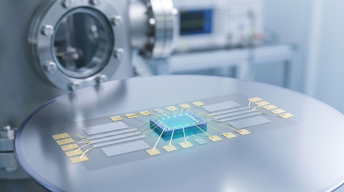
The demand for high-performance, low-power radio frequency (RF) components is relentless. From 5G communications to advanced radar systems, the ability to actively tune the properties of filters, attenuators, and oscillators is a critical engineering challenge. Traditional methods often rely on bulky magnetic coils or inefficient thermal tuning. A new frontier in materials science, however, offers a more elegant solution: using an electric field to control magnetism at the atomic scale.
This guide translates a cutting-edge theoretical proposal into a tangible laboratory prototype. Based on research by Cvitkovich, Zollner, and Fabian, we will outline the steps to build and test a voltage-controlled microwave filter using a heterostructure of graphene and an emerging 2D magnet, Fe$_3$GeTe$_2$ (FGT). The core principle is the electrical tuning of magnetic damping, a fundamental property that governs how a magnetic material dissipates energy. By controlling this property with a simple gate voltage, we can create a new class of highly efficient, tunable spintronic devices. This exploration is a prime example of advanced graphene electronics.
Our goal is to construct a solid-state device where the attenuation of a microwave signal can be modulated by a DC voltage. The prototype consists of three main parts:
1. A Coplanar Waveguide (CPW): This is a standard structure for guiding microwave signals on a chip. It consists of a central signal line flanked by two ground planes.
2. An Active Heterostructure: A small flake of the 2D ferromagnet FGT is placed on top of a sheet of monolayer graphene. This FGT/graphene stack is the heart of the device.
3. A Gating Structure: The graphene layer and a doped silicon substrate act as the two plates of a capacitor, with a thin layer of silicon dioxide as the insulator. Applying a voltage between them creates an electric field that tunes the active region.
The device operates based on the principle of ferromagnetic resonance (FMR). When a microwave signal travels down the CPW, its oscillating magnetic field interacts with the FGT. If the microwave frequency matches the FGT's natural resonant frequency (which is set by an external static magnetic field), the FGT will strongly absorb energy from the signal. This absorption creates a dip in the transmitted signal, effectively filtering out that specific frequency.
The innovation here is controlling the characteristics of that absorption. The research shows that the magnetic damping of the FGT/graphene stack can be changed by orders of magnitude with a gate voltage.
- Low Damping State: The FMR absorption is very sharp and narrow. The device acts as a narrowband notch filter.
- High Damping State: The FMR absorption becomes very broad and shallow. The device acts as a broadband attenuator.
By simply adjusting the DC gate voltage, we can switch the device between these states, creating a tunable RF component with no moving parts and minimal power consumption for the control signal.
This practical guide is based on the 2026 theoretical paper "Gate-tunable magnetic damping in van der Waals Heterostructures" by Cvitkovich, Cvitkovich, and Fabian. Their work provides the foundational physics for our prototype. It is important to note that their findings are based on first-principles density functional theory (DFT) calculations, not a physical experiment. Our guide aims to be the bridge from their theory to experimental validation.
The key findings from the source are:
1. Mechanism of Damping: In materials like FGT, magnetic damping is heavily influenced by the electronic band structure, specifically near points where electron energy bands approach each other due to spin-orbit coupling. The authors call these "spin hot spots."
2. Role of the Fermi Level: The amount of damping depends on the position of the Fermi level (the energy level up to which electron states are filled) relative to these spin hot spots. If the Fermi level sits right on a hot spot, damping is high. If it is moved away, damping drops significantly.
3. Gating Effect: In an FGT/graphene heterostructure, an out-of-plane electric field (created by our gate voltage) can effectively shift the energy bands. This allows for precise electrical control over the Fermi level's position relative to the hot spots.
4. Magnitude of Change: The calculations predict that this gating mechanism can modulate the magnetic damping over several orders of magnitude. This is a giant effect, promising a high on/off ratio for any resulting device.
Our engineering guide takes this theoretical model and proposes a specific device architecture, a plausible fabrication workflow, and a test plan to verify the predictions. The device geometry, material choices beyond FGT/graphene, and process parameters are engineering assumptions based on common practices in the fields of 2D materials and microwave engineering.
Building this prototype requires access to a cleanroom environment with nanofabrication and characterization tools.
Materials:
- Substrate: A 4-inch high-resistivity silicon wafer with a 285 nm or 300 nm thermally grown silicon dioxide (SiO$_2$) layer. The doped silicon serves as the back gate electrode.
- Graphene: High-quality monolayer graphene grown by chemical vapor deposition (CVD) on a copper foil.
- 2D Ferromagnet: A bulk crystal of Iron Germanium Telluride (Fe$_3$GeTe$_2$). These are commercially available from specialist suppliers.
- Chemicals: Acetone, isopropyl alcohol (IPA), photoresist, developer, and buffered oxide etchant (BOE) for cleaning and lithography.
- Metal Targets: High-purity titanium (Ti) and gold (Au) for creating the electrical contacts and waveguide.
Fabrication Equipment:
- Optical Lithography System: A mask aligner for patterning micron-scale features. For higher precision, an electron-beam lithography system would be superior.
- Metal Deposition System: A thermal or e-beam evaporator to deposit thin metal films.
- Reactive Ion Etcher (RIE): For plasma cleaning and potentially patterning steps.
- Dry Transfer Station: A microscope-equipped station with micromanipulators for picking up and placing 2D material flakes. This is a critical piece of equipment.
- Wire Bonder: For making electrical connections from the chip to a larger circuit board.
- Optical Microscope: For identifying and aligning 2D material flakes.
Test Equipment:
- Cryogenic Probe Station: FGT is ferromagnetic below its Curie temperature of approximately 220 K (-53 C). Therefore, all testing must be performed at low temperatures.
- Vector Network Analyzer (VNA): For measuring microwave signal transmission (S-parameters) up to at least 20 GHz.
- DC Voltage Source: A precise source-measure unit (SMU) or low-noise DC supply for applying the gate voltage.
- Electromagnet: A magnet capable of providing a stable, controllable out-of-plane magnetic field.
This process involves the careful assembly of different materials at the micro-scale. Precision and cleanliness are paramount.
1. Substrate Preparation:
- Dice the Si/SiO$_2$ wafer into smaller pieces (e.g., 1 cm x 1 cm).
- Clean the chips thoroughly using a standard solvent cleaning process (acetone, then IPA).
- Perform a gentle oxygen plasma clean in the RIE for a few seconds to remove any organic residue and prepare the surface.
2. Graphene Transfer:
- Transfer the CVD graphene from its native copper foil to one of the prepared Si/SiO$_2$ chips. A standard PMMA-assisted wet transfer process can be used.
- After transfer, anneal the chip in a vacuum or forming gas environment to remove polymer residue and improve the graphene-substrate interface.
3. FGT Exfoliation and Transfer:
- Use the mechanical exfoliation method, famously known as the "Scotch tape method," to cleave thin flakes from the bulk FGT crystal.
- Press the tape onto a separate, clean Si/SiO$_2$ chip. The thin flakes will adhere to the substrate.
- Using an optical microscope, identify monolayer or few-layer FGT flakes. They will have a distinct optical contrast. The source paper focuses on monolayer FGT, so aim for the thinnest, most uniform flakes possible.
- Using the dry transfer station, pick up a suitable FGT flake and carefully align and place it onto the graphene layer on your device chip. This creates the FGT/graphene heterostructure.
4. Waveguide and Contact Patterning:
- Spin-coat a layer of photoresist over the entire chip.
- Use the mask aligner to expose the resist with a photomask that defines the coplanar waveguide and the contact pads. The central signal line of the CPW should be designed to pass directly over the FGT/graphene stack. A typical signal line width might be 10-20 micrometers.
- Develop the resist, leaving a patterned stencil for metal deposition.
5. Metal Deposition:
- Place the chip in the metal evaporator.
- Deposit an adhesion layer of titanium (e.g., 5 nm) followed by a conductive layer of gold (e.g., 80-100 nm).
- Perform a lift-off process by immersing the chip in acetone. The resist will dissolve, taking the overlying metal with it and leaving only the desired metal waveguide and contacts.
6. Device Packaging:
- Mount the finished chip onto a custom printed circuit board (PCB) designed with matching microwave connectors.
- Use the wire bonder to connect the on-chip contact pads (for the CPW and the back gate) to the corresponding pads on the PCB.
The test plan is designed to directly measure the gate-tunable magnetic damping predicted by the source research.
1. Setup:
- Mount the packaged device inside the cryogenic probe station and cool it down to a stable temperature well below FGT's Curie temperature (e.g., 77 K or 10 K).
- Connect the VNA to the CPW ports on the PCB.
- Connect the DC voltage source to the back gate contact. The ground will be common with the CPW ground planes.
- Position the electromagnet to apply a static magnetic field perpendicular to the plane of the chip.
2. Measurement Procedure:
- Set the external magnetic field to a fixed value (e.g., 0.1 Tesla).
- Set the gate voltage (V_g) to 0 V.
- Perform a frequency sweep with the VNA, measuring the S21 transmission parameter. Record the data. You should observe an absorption dip at the FMR frequency.
- Increment the gate voltage. The source does not specify a voltage range, so a cautious approach is needed. Start with a sweep from -40 V to +40 V in 5 V steps. This range is typical for gating graphene on a 300 nm SiO$_2$ dielectric.
- Repeat the VNA frequency sweep at each gate voltage step.
- If the effect is observed, perform a finer sweep around the voltages that show the most significant change.
3. Data Analysis and Expected Results:
- Plot the S21 transmission (in dB) versus frequency for each gate voltage.
- You should see that the absorption dip's shape changes dramatically with V_g.
- For each curve, extract the FMR linewidth, which is the full width at half maximum (FWHM) of the absorption peak. The linewidth is directly proportional to the magnetic damping.
- The primary result will be a plot of FMR linewidth versus gate voltage.
- Based on the source, you should expect to see a non-monotonic behavior. At certain gate voltages, the linewidth should be very small (low damping). At other voltages, where the Fermi level aligns with a spin hot spot, the linewidth should increase dramatically, potentially by a factor of 100 or more. This would be a direct experimental confirmation of the theory.
Translating theory into a working device is fraught with challenges. Awareness of these risks is key to success.
- Material and Interface Quality: The entire concept relies on a clean, electronically well-behaved interface between the graphene and the FGT. Any contamination, polymer residue, or structural defects can introduce scattering that masks the desired effect. This is the single greatest risk.
- Fabrication Tolerances: The alignment of the FGT flake, graphene, and the metallic waveguide is critical. Misalignment can lead to poor signal coupling and unreliable results.
- Operating Temperature: The need for cryogenic operation is a significant practical limitation for many applications. While FGT was used in the model, this principle could apply to other 2D magnets with higher Curie temperatures as they are discovered.
- Missing Parameters: The source paper does not specify the exact gate voltage required. The actual voltage will depend on the quality of the dielectric, the charge carrier density in the graphene, and the specific band alignment of the fabricated stack. Experimentation is required.
- Scalability: This guide uses mechanically exfoliated flakes, which is a method suitable only for research and prototyping. For any commercial graphene applications, a scalable manufacturing process would be needed. This would involve developing techniques for large-area growth of high-quality FGT/graphene heterostructures, a significant challenge in graphene manufacturing techniques.
Despite these challenges, this prototype represents a fascinating step toward a new generation of spintronic devices. Successfully demonstrating electrical control over magnetic damping would validate a powerful physical principle and open the door to developing ultra-low-power, compact, and tunable components for a wide range of high-frequency electronics.
Serious about B2B integration? Test our premium Pulsed Electrical Resistive Carbon Heating turbostratic graphene in your lab. 100g sample packs available now.
Explore More
Researchers map ballistic transport in bilayer graphene junctions, revealing quantized conductance thresholds. This fundamental work is key to designing...

Discover the importance of physisorbed metal nanoparticles and their contact mechanics. This research explores how Al and Cu particles interact on a nanoscale.

Learn to build a prototype graphene Josephson junction. This guide details how to use proximity-induced superconductivity for next-gen quantum devices.