
3D Atomic Imaging of Graphene Dynamics from a Single Low-Dose TEM Snapshot
A new physics-informed AI method reconstructs the 3D atomic structure and dynamics of graphene from a single low-dose TEM image, solving a key imaging...
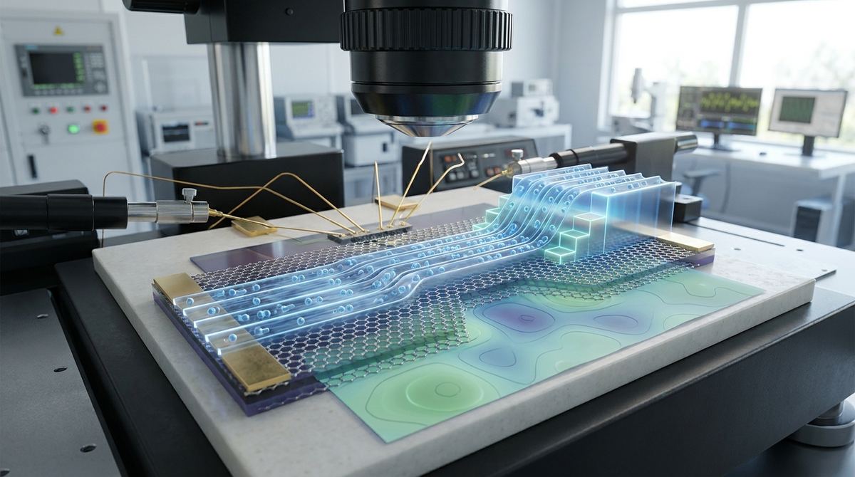
Imagine driving on a futuristic highway where new lanes magically appear only when your car reaches specific speeds. At 50 miles per hour, you have two lanes. But the moment you hit 60, a third lane opens up, instantly increasing the flow of traffic. This is a surprisingly accurate analogy for how electrons can behave inside advanced nanomaterials. In the quantum world of bilayer graphene, electrons don't just flow smoothly; their ability to travel, known as conductance, can jump up in discrete, predictable steps. Understanding the rules of this quantum highway is essential for engineering the next generation of computer chips that are faster, smaller, and vastly more energy-efficient than anything we use today.
For decades, the electronics industry has been driven by our ability to shrink silicon transistors, packing more and more processing power into smaller spaces. However, we are rapidly approaching the fundamental physical limits of silicon. At the nanoscale, quantum effects begin to dominate, and the reliable, predictable behavior of silicon starts to break down. This has spurred a global search for new materials to build the logic gates and switches of future computers. Bilayer graphene, a material made of two stacked sheets of single-atom-thick carbon, is a leading contender. Unlike its single-layer counterpart, its electronic properties can be tuned with an electric field, allowing engineers to create a bandgap, which is crucial for turning a transistor "off."
The problem is that while we know bilayer graphene has potential, we lack a complete, predictive understanding of how electrons travel through it, especially in the complex environment of a junction—the core of a transistor. Without a precise map of electron behavior, designing devices is like navigating a maze blindfolded. Engineers need to know exactly how conductance changes with applied voltage and how the material's unique electronic structure, with its multiple energy bands, contributes to the overall flow of current. Before we can build reliable bilayer graphene electronics, we must answer a fundamental question: what are the precise rules governing electron transport at the quantum level? A recent theoretical study by Dan-Na Liu, Jun Zheng, and Pierre A. Pantaleon provides a critical piece of this puzzle.
The central idea behind the research is to dissect the flow of electrons through a bilayer graphene junction into its most basic components. Instead of viewing the electrical current as a single, uniform river, the researchers treated it as a collection of separate streams, each corresponding to a different quantum "mode" or channel available for transport. This is known as a "mode-resolved" approach. Each of these modes is linked to one of the specific energy "bands" in bilayer graphene's electronic structure. These bands are like predefined energy levels that electrons are allowed to occupy.
By modeling the system this way, the researchers could calculate how much each individual mode contributes to the total conductance. More importantly, they could predict the exact energy (which can be controlled by a voltage) at which a new mode becomes available for electrons to travel through. The moment a new mode opens up, the total conductance of the junction jumps up by a discrete amount. This sudden increase is a "conductance threshold." The research, therefore, creates a detailed theoretical roadmap that connects the fundamental electronic structure of bilayer graphene directly to the measurable electrical properties of a device built from it. It moves beyond simple observation to provide a powerful predictive tool for nanoelectronic design.
The system at the heart of this study is a theoretical model of a bilayer graphene junction. Bilayer graphene consists of two layers of the familiar hexagonal carbon lattice, stacked in a specific arrangement known as Bernal stacking. This stacking is critical, as it gives rise to a more complex and useful electronic band structure than that of single-layer graphene. While single-layer graphene has no bandgap, making it difficult to use in digital switches, an electric field applied perpendicular to the bilayer sheets can open one up. This allows the material to be switched from a conducting "on" state to an insulating "off" state.
The "junction" in the model is a conceptual device where such an electric field is applied to a small, defined region. This creates an energy barrier that electrons must overcome. The researchers' work simulates what happens when electrons with varying amounts of energy approach this junction. Their model assumes a scenario of "ballistic transport," which is the ideal limit of electron flow. In this regime, electrons travel through the material without scattering off impurities, defects, or thermal vibrations, much like a bullet flying through a vacuum. While this is an idealization, it reveals the absolute maximum performance of the material and its intrinsic quantum properties. The calculations likely use established quantum transport formalisms to determine the probability that an electron will pass through the junction, which directly translates to the electrical conductance.
The primary discovery of the research is the precise, quantitative mapping of these conductance thresholds. The model predicted that as the energy of the electrons is increased, the conductance of the bilayer graphene junction does not rise smoothly. Instead, it increases in a series of sharp, well-defined steps. Each step signifies the opening of a new quantum channel for electron transport. The researchers were able to resolve these steps and attribute each one to the activation of a specific mode originating from one of the material's distinct electronic bands.
They demonstrated how the height and position of these conductance steps are directly dependent on the properties of the junction, such as its width and the strength of the applied electric field used to create the bandgap. This provides a clear set of rules for how to tune the device to achieve desired electrical characteristics. For instance, a stronger electric field might shift the energy at which a certain threshold appears. This detailed, mode-resolved picture confirms that the different electronic bands in bilayer graphene contribute to transport in unique and separable ways, offering a new level of control for device engineers. The findings effectively provide a quantum fingerprint of electron transport in these advanced junctions.
This work is significant because it transforms our understanding of bilayer graphene from a qualitative appreciation of its potential to a quantitative, predictive science. For engineers aiming to build the next wave of graphene electronics, this theoretical roadmap is invaluable. It eliminates much of the guesswork involved in device design. Instead of relying on costly and time-consuming trial-and-error fabrication, designers can use this model to predict how a junction with specific dimensions and applied voltages will behave.
This level of predictive power is crucial for creating complex integrated circuits. Knowing the exact location of conductance thresholds allows for the design of digital switches that operate with minimal energy. A transistor could be biased to sit just below a threshold, requiring only a tiny nudge in voltage to jump to a higher conductance "on" state. This could lead to logic gates with dramatically lower power consumption and higher switching speeds compared to their silicon counterparts. The research provides the fundamental physics foundation upon which practical, high-performance electronic applications can be built, bridging the gap between abstract quantum theory and tangible engineering specifications.
It is crucial to recognize the context and limitations of this research. The study is purely theoretical and relies on a highly idealized model. The assumption of ballistic transport, while essential for isolating the intrinsic quantum effects, does not reflect the reality of most fabricated devices. In the real world, electrons inevitably scatter off imperfections in the graphene lattice, impurities from the manufacturing process, and thermal vibrations of the atoms. This scattering reduces conductance and can smear out the sharp, quantized steps predicted by the model.
Therefore, the most critical next step is experimental validation. Fabricating pristine bilayer graphene junctions that approach the ballistic limit is an immense technical challenge. It requires atomically precise manufacturing techniques to create clean interfaces and high-quality material. Experimentalists will need to measure the conductance of these devices at very low temperatures to minimize thermal scattering and see if the predicted step-like features emerge. Furthermore, the model likely uses simplified geometries. Real-world devices will have more complex shapes and edge effects that could influence transport properties. Future theoretical work will need to incorporate these more realistic factors to create models that are even more applicable to practical engineering.
While this research will not lead to a new product tomorrow, it lays the essential groundwork for numerous future technologies. The most direct application is in the design of post-silicon digital logic. The ability to precisely control conductance states in bilayer graphene transistors could enable ultra-low-power processors for everything from mobile devices to massive data centers. Beyond conventional computing, these principles could be applied to high-frequency electronics for 6G communications and beyond, where the high mobility of electrons in graphene is a major advantage.
The discrete nature of the conductance steps also hints at applications in quantum devices. A junction could potentially be configured to operate with only a few conducting modes, making it a building block for quantum computing components or highly sensitive detectors. By understanding exactly how to open and close these quantum channels, researchers can engineer devices that exploit these fragile quantum effects. The insights gained are fundamental to leveraging the full potential of high-quality graphene, such as that found in turbostratic graphene flakes, for any application that depends on pristine electronic transport.
If you take away just one idea from this research, let it be this: electron flow through a bilayer graphene junction is not a simple, continuous process. It is a quantum phenomenon that occurs in discrete, predictable steps. This work provides the first detailed map of these steps, showing how they are tied directly to the material's fundamental electronic structure and can be controlled by an electric field, giving engineers a new and powerful blueprint for designing future electronic devices.
What is bilayer graphene?
Bilayer graphene is a two-dimensional material composed of two sheets of carbon atoms arranged in a hexagonal lattice, stacked one on top of the other. Unlike single-layer graphene, its electronic properties, particularly its bandgap, can be dynamically tuned by applying an external electric field. This tunability makes it a highly promising candidate for building semiconductor components like transistors.
What is ballistic transport?
Ballistic transport is an idealized form of electrical conduction where electrons travel through a material without being scattered or deflected by imperfections, impurities, or vibrations in the material's atomic lattice. It represents the most efficient possible flow of charge and reveals the intrinsic quantum properties of a material's conductance. This phenomenon typically occurs over very short distances in ultra-clean materials at low temperatures.
Why is a bandgap important for transistors?
A bandgap is a range of energy levels that electrons are forbidden from occupying within a material. Materials with a bandgap, like silicon, are called semiconductors. This property is essential for a transistor because it allows the device to be turned "off." By applying a voltage, you can move the available energy levels for electrons out of the conducting range and into the bandgap, effectively stopping the flow of current and creating a digital '0'.
What is a "conductance threshold" in this context?
A conductance threshold is a specific energy or voltage level at which the electrical conductance of the bilayer graphene junction suddenly jumps to a higher value. This jump occurs because the increased energy allows electrons to access a new quantum channel, or "mode," for transport through the device. The conductance increases in a step-like fashion at each of these thresholds rather than rising smoothly.
Is this technology ready to be used in commercial products?
No, this technology is still in the early, fundamental research stage. The study presents a theoretical model that needs to be validated by complex experiments. Furthermore, the manufacturing challenges of producing large-scale, defect-free bilayer graphene junctions suitable for integrated circuits are significant. While the findings are a crucial step forward, it will likely be many years before these principles are incorporated into consumer electronics.
The work by Dan-Na Liu, Jun Zheng, and Pierre A. Pantaleon provides a profound look into the quantum mechanics that govern the flow of electricity in bilayer graphene junctions. By resolving the individual transport modes and mapping the precise conductance thresholds, they have created an essential theoretical framework for the future of nanoelectronics. This research illuminates the path from understanding a material's exotic properties to engineering its function. While the road from theoretical model to commercial reality is long, this detailed map of bilayer graphene's quantum highway is an indispensable guide for navigating the challenges and unlocking the potential of carbon-based electronics.
Serious about B2B integration? Test our premium Pulsed Electrical Resistive Carbon Heating turbostratic graphene in your lab. 100g sample packs available now.
Explore More
A new physics-informed AI method reconstructs the 3D atomic structure and dynamics of graphene from a single low-dose TEM image, solving a key imaging...

Explore how to build a graphene-FGT voltage-tuned microwave filter. This guide details a prototype for electrically controlling magnetic damping in spintronics.

Discover the importance of physisorbed metal nanoparticles and their contact mechanics. This research explores how Al and Cu particles interact on a nanoscale.