
A New Era of Graphene Engineering: Pre-Designing Twist Angles on Demand
Researchers have developed a breakthrough method for growing twisted bilayer graphene with pre-designed angles, a key step toward manufacturable quantum...
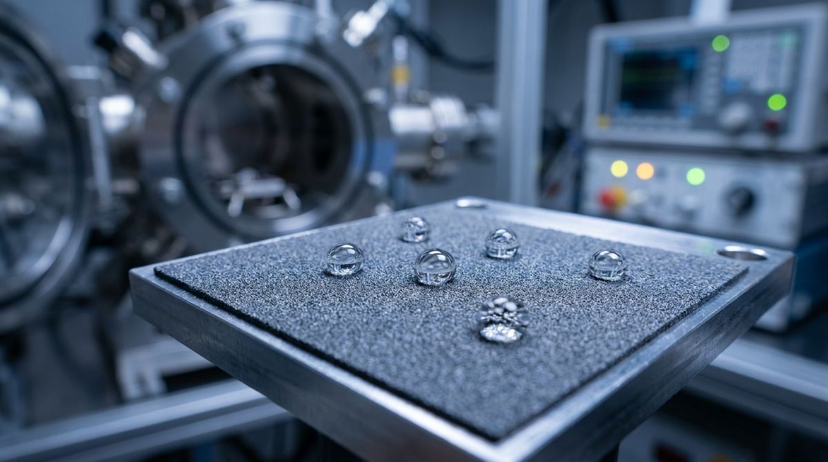
For engineers developing microfluidic devices, biofouling and non-specific adsorption are persistent hurdles. When complex fluids like blood, serum, or oils move through micro-channels, they tend to adhere to the channel walls. This leads to sensor drift, clogging, and inconsistent flow rates. Traditional coatings often fail because they rely on chemical hydrophobicity, which can be overcome by surfactants or high-pressure flows.
The research from Nunez Galvez et al. (2026) suggests a structural solution rather than a purely chemical one. By creating a hierarchical architecture—specifically graphene nanowalls (GNWs) grown on top of metal oxide nanotubes—we can create a surface that is omniphobic. This means it repels not just water, but also complex biological fluids and oils, achieving contact angles exceeding 170 degrees.
The core technology involves a 2D-3D hybrid structure. The 3D component is a scaffold of metal oxide nanotubes (such as TiO2, Al2O3, or SiO2). The 2D component is the graphene nanowall.
When graphene grows conformally over these nanotubes, it creates a re-entrant surface geometry. This geometry is the secret to superwettability. The roughness at multiple scales (the nanotubes and the graphene sheets) traps air pockets, preventing the liquid from ever truly touching the solid surface. This is the "Lotus Effect" scaled for complex fluids. Unlike standard coatings, this structure is robust and can maintain its repellency even under UV irradiation or condensation.
The most immediate practical application for a startup or lab is the development of anti-fouling coatings for microfluidic sensor channels. If you are building a point-of-care diagnostic chip that must process whole blood or serum, using this graphene-oxide architecture can ensure that the fluid flows through the channel without leaving protein residue on the walls.
This application is particularly valuable for:
1. Lab-on-a-chip devices requiring high sensitivity.
2. Micro-scale oil-water separation systems.
3. Self-cleaning optical windows in micro-environments.
4. Bio-sensors that must operate in high-humidity or condensation-prone environments.
To replicate this process in a lab or pilot production setting, you will need the following:
1. Oxide Nanotube Scaffolds: TiO2, Al2O3, or SiO2 nanotubes. These serve as the 3D template.
2. Organic Template: Single-crystalline organic nanowires. These are used to guide the initial growth and ensure the vertical orientation of the nanotubes.
3. Carbon Source: A hydrocarbon gas, typically Methane (CH4) mixed with Hydrogen (H2).
4. Plasma-Enhanced Chemical Vapor Deposition (PECVD) System: A reactor capable of low-pressure, plasma-assisted growth.
5. Characterization Tools: Scanning Electron Microscopy (SEM) for morphology, Raman Spectroscopy for graphene quality, and a Contact Angle Goniometer for wetting tests.
The following process is an engineering implementation based on the research methodology. Because the exact plasma parameters are proprietary to the research group, the values provided here are cautious starting ranges for a laboratory setting.
1. Substrate Preparation and Templating
Begin with your chosen metal oxide nanotube scaffold. If you are growing the nanotubes from scratch, you must first deposit the single-crystalline organic nanowires. These act as the 1D soft template.
2. Plasma-Assisted Oxide Deposition
Using the PECVD system, deposit the metal oxide (e.g., TiO2) over the organic template.
Assumed Parameters:
- Temperature: 200C to 350C (must remain low enough to prevent premature degradation of the organic template).
- Pressure: 1 to 10 Torr.
- Power: Low RF power to ensure conformal coating without destroying the template.
3. Graphene Nanowall (GNW) Growth
Once the oxide scaffold is established, introduce the carbon source (CH4/H2). The plasma will dissociate the methane, allowing the carbon to grow as vertically oriented nanowalls on the oxide nanotubes.
Assumed Parameters:
- Temperature: 300C to 450C.
- Gas Ratio: 1:4 (CH4 to H2) as a starting point.
- Vacuum: Low vacuum conditions (mTorr range).
4. Post-Growth Stabilization
A brief thermal annealing step in an inert atmosphere (Argon) may be required to stabilize the sp2 graphitic framework and ensure the edge functionalization is controlled.
To ensure your prototype meets the requirements for omniphobicity, follow this testing plan:
1. Morphological Verification
Use SEM to confirm that the graphene nanowalls are radially oriented and conformally cover the nanotubes. The surface should look like a dense, dark forest of needles. Use TEM to verify the interface between the graphene and the oxide.
2. Wetting Analysis
Perform contact angle measurements using a goniometer.
- Test with deionized water (target > 150 degrees).
- Test with bovine serum or a similar complex biological fluid (target > 170 degrees).
- Test with a non-polar liquid like hexadecane to confirm omniphobicity.
3. Structural Integrity
Use Raman Spectroscopy to check the G and 2D peaks. You are looking for a strong sp2 signal, which confirms the graphene is high quality. Check for the presence of edge functionalization, which helps in tuning the surface energy.
4. Environmental Durability
Expose the surface to UV light for 24-48 hours and observe any changes in wetting behavior. Test the surface under high humidity to ensure condensation does not lead to liquid infiltration into the pores.
The transition from a research paper to a physical prototype involves several risks:
- Template Stability: The research relies on organic nanowires as a template. In a production environment, maintaining the integrity of these organic wires during the oxide deposition and plasma growth phases is the most significant challenge. If the temperature exceeds the decomposition point of the template, the hierarchical structure will collapse.
- Plasma Etching vs. Growth: Plasma is a double-edged sword. While it enables low-temperature growth, excessive power or long exposure can etch the oxide nanotubes or the graphene itself, destroying the re-entrant geometry required for omniphobicity.
- Scalability: While the paper describes a scalable route, PECVD is traditionally a batch process. Scaling this to large-area microfluidic wafers requires highly uniform plasma distribution across the entire substrate.
- Assumption on Gas Ratios: The exact CH4/H2 ratios and plasma power settings are not explicitly detailed in the source. The values provided are engineering assumptions intended to prevent substrate damage.
This guide is based on the research findings of Nunez Galvez et al. (2026). The core discovery—that GNWs can decouple surface behavior from the intrinsic chemistry of the oxide—is the primary technical driver for this application.
Note that while the research demonstrates success with TiO2, Al2O3, and SiO2, the specific performance of the coating will vary depending on the oxide chosen. For example, TiO2 offers additional photocatalytic properties which may be beneficial for self-cleaning applications, whereas Al2O3 may offer superior mechanical stability.
Serious about B2B integration? Test our premium Pulsed Electrical Resistive Carbon Heating turbostratic graphene in your lab. 100g sample packs available now.
Explore More
Researchers have developed a breakthrough method for growing twisted bilayer graphene with pre-designed angles, a key step toward manufacturable quantum...

Learn how deep learning is revolutionizing the structural characterization of twisted bilayer materials, accelerating the development of next-generation...

Learn to build a prototype graphene FET biosensor for sensitive DNA detection. This guide covers materials, fabrication, and testing for point-of-care...