
Rippled Graphene Pores for Neuromorphic Fluidic Memristive Devices
Discover how rippled graphene pores act as fluidic memristors, enabling advanced synaptic functionalities for the next generation of neuromorphic computing.
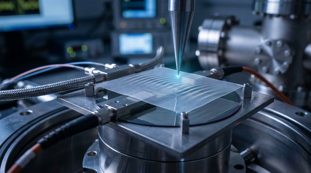
The research by Bahamondes, Soto-Garrido, Muñoz, and Juričić (2026) describes a fundamental coupling between the mechanical ripples (flexural phonons) and the electronic states (Dirac fermions) in crystalline membranes like graphene. Specifically, they identify a critical point where these two systems lock together, creating a hybrid electronic-structural state. For an engineer, this represents a roadmap for a new class of devices: the strain-modulated electronic switch.
In traditional field-effect transistors (FETs), we use a gate voltage to shift the Fermi level and control conductivity. In a ripple-modulated switch, we use controlled mechanical deformation to shift the Dirac point. By inducing specific ripple patterns, we can effectively turn the current on or off by altering the electronic band structure through structural geometry. This approach offers a potential path toward ultra-fast, high-sensitivity sensing and switching that operates at the intersection of mechanical and electronic domains.
To realize this, we cannot use graphene sitting flat on a substrate. The physics described in the research requires a suspended membrane to allow for the flexural modes (ripples) to exist without being damped by the substrate.
The proposed device is a micro-electromechanical system (MEMS) consisting of a suspended graphene sheet positioned over a piezoelectric actuator. By applying a voltage to the piezo, we induce a controlled ripple pattern in the graphene. This mechanical deformation changes the local strain, which, according to the research, couples directly to the Dirac fermions, allowing us to modulate the electrical resistance of the sheet.
To build a functional prototype, the following materials are required:
- High-quality CVD Graphene: Single-layer graphene grown on copper foil via chemical vapor deposition. High carrier mobility is essential for observing the Dirac fermion response.
- Substrate: A silicon wafer with a thick SiO2 layer (approximately 300nm) to provide electrical isolation.
- Actuator: A Lead Zirconate Titanate (PZT) thin film or a macro-scale piezo element. For a micro-scale prototype, a PZT layer integrated directly beneath the suspended membrane is ideal.
- Electrodes: Gold (Au) for the primary contact pads and Titanium (Ti) as an adhesion layer.
- Transfer Medium: PMMA (Polymethyl methacrylate) for the graphene transfer process.
- Etchant: Hydrofluoric acid (HF) or buffered oxide etch (BOE) to create the necessary cavities in the SiO2.
1. Substrate Preparation: Fabricate a cavity in the SiO2/Si substrate using photolithography and reactive ion etching. The cavity depth should be between 50nm and 100nm to allow the graphene to hang freely without touching the bottom of the trench.
2. Electrode Patterning: Use electron-beam lithography to define the contact areas on the edges of the cavity. Deposit Ti/Au via electron-beam evaporation. The contacts must be robust enough to maintain electrical connection even when the membrane is under mechanical stress.
3. Graphene Transfer: Use the PMMA-assisted transfer method. Spin-coat PMMA onto the CVD graphene, etch the copper growth substrate, and then float the PMMA/graphene onto the target substrate. Ensure the graphene is centered over the cavity.
4. Actuator Integration: Deposit a piezoelectric layer (such as PZT) in the cavity area or integrate a piezo-actuator that applies mechanical stress to the edges of the suspended membrane. The goal is to induce periodic strain rather than uniform tension.
5. Cleaning and Annealing: Perform a careful PMMA removal process using acetone. Follow this with a thermal anneal in a hydrogen/argon (H2/Ar) atmosphere at approximately 300 degrees Celsius to remove residual polymers and improve contact resistance.
To verify that the mechanical ripples are successfully modulating the electronic states, the following tests should be performed:
- Electrical Transport Measurements: Use a four-probe setup to measure the I-V characteristics of the graphene. The primary metric is the shift in the charge neutrality point (the Dirac point) as the piezo voltage is varied. A successful device will show a measurable change in resistance at a fixed gate voltage as the piezo induces ripples.
- Raman Spectroscopy: Use Raman mapping to correlate the electronic shifts with the physical ripple pattern. The G-peak and 2D-peak positions are highly sensitive to local strain. By mapping these peaks, you can visualize whether the induced ripples match the wavelength predicted by the theory.
- Atomic Force Microscopy (AFM): Use AFM in tapping mode to visualize the topography of the ripples. Note that the wavelength of these ripples may be extremely small, potentially requiring high-resolution AFM with a specialized probe.
- Frequency Response Testing: Measure the electrical response time relative to the mechanical actuation frequency. This will determine if the device can operate at the high speeds suggested by the relativistic-like dynamics of the Dirac fermions.
The research provides the theoretical framework, but several assumptions must be made for a physical prototype:
- Ripple Control: The research discusses specific momentum modes (Q and -Q). In a real-world engineering environment, we assume that a piezoelectric actuator can induce these specific periodic modes rather than just random thermal noise or uniform tension.
- Material Quality: We assume the CVD graphene is sufficiently clean and has high enough carrier mobility to allow the Dirac fermions to respond clearly to the strain.
- Scale: The research discusses the continuum limit. We assume that a MEMS-scale device (micrometer scale) will sufficiently capture the physics described in the field theory.
- Membrane Rupture: The most significant risk is the graphene tearing during the transfer process or under high piezo voltage. Mitigation: Use low-voltage, incremental testing and ensure the graphene is of high structural integrity.
- Thermal Drift: Mechanical and electrical measurements are highly sensitive to temperature changes. Mitigation: Perform all tests in a temperature-controlled environment or a vacuum chamber to stabilize the thermal environment.
- Stochastic Rippling: Natural thermal ripples may interfere with the controlled ripples. Mitigation: The device may need to be operated at lower temperatures or higher actuation voltages to ensure the controlled, engineered mode dominates the energy landscape.
This guide is based on the theoretical findings of Bahamondes, Soto-Garrido, Muñoz, and Juričić (2026) regarding the coupling of flexural phonons and Dirac fermions in crystalline membranes. Specifically, it utilizes the concept of the hybrid electronic-structural critical point and the chiral-XY Gross-Neveu-Yukawa universality class to justify the use of mechanical strain as a control mechanism for electronic states.
Serious about B2B integration? Test our premium Pulsed Electrical Resistive Carbon Heating turbostratic graphene in your lab. 100g sample packs available now.
Explore More
Discover how rippled graphene pores act as fluidic memristors, enabling advanced synaptic functionalities for the next generation of neuromorphic computing.

Learn how to use electromechanical responses in gapped graphene to measure electronic temperature and band gaps using traveling flexural waves.

Explore how researchers have discovered viscous electron fluid behavior in cadmium, a breakthrough that could revolutionize the future of nanoelectronics.