
Practical Guide: A Practical Guide to Building a Graphene Battery Safety Sensor
Build a flexible graphene battery sensor for real-time temperature and strain monitoring, a crucial step toward preventing thermal runaway in Li-ion cells.
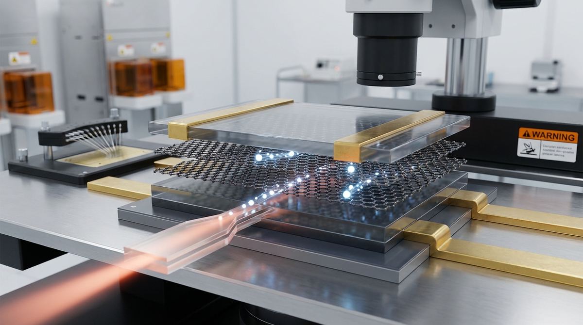
The modern digital world relies on a silent, invisible torrent of light traveling through fiber-optic cables. Every time you stream a high-definition video, send a massive email attachment, or engage in a high-frequency financial transaction, you are relying on photodetectors that convert light into electrical signals. As our demand for data grows, the hardware responsible for this conversion is hitting a physical wall. Current technologies struggle to keep up with the blistering speeds required by next-generation networks, often forced to choose between being fast and being sensitive. However, a recent breakthrough in graphene engineering suggests that we may soon bypass these physical constraints entirely, ushering in an era of ultra-fast, energy-efficient communication.
In the realm of optical communications, researchers face a fundamental obstacle known as the responsivity-bandwidth trade-off. To understand this, one must look at how a photodetector captures light. When a photon hits a semiconductor, it knocks an electron loose, creating a charge carrier. To turn this into a signal, these carriers must be collected by electrodes. Responsivity refers to how much electrical current is generated for a given amount of light; high responsivity requires a thick enough material to ensure most photons are absorbed. Bandwidth, on the other hand, refers to how quickly the device can reset itself to detect the next pulse of light. High bandwidth requires a very thin material so that the charge carriers have a very short distance to travel before being collected.
This creates a direct conflict. If you make the material thicker to catch more light (high responsivity), the carriers take too long to travel through the material, which slows down the device (low bandwidth). If you make the material thinner to increase speed, most photons pass right through without being absorbed, resulting in a very weak signal (low responsivity). Furthermore, most high-speed detectors require an external voltage, known as a bias, to pull the carriers toward the electrodes. This external voltage introduces thermal noise and consumes significant power, which is problematic for massive data centers that consume enormous amounts of electricity.
The solution proposed by the researchers involves a concept called heterostructure engineering. Instead of using a single, thick chunk of semiconductor material, the team built a microscopic sandwich of different 2D materials. Imagine a single sheet of graphene—a material only one atom thick—sandwiched between other ultra-thin layers of crystals. This sandwich does not just provide a path for light; it creates an internal, built-in electric field.
This internal field acts like a high-speed slide for electrons. As soon as light hits the graphene and creates charge carriers, the internal field immediately pushes them in opposite directions. Because the movement is driven by an internal force rather than an external power source, the device can operate at zero-bias, meaning it requires no external voltage to function. This architecture allows the device to be incredibly thin, which ensures high speed, while the engineered layers ensure that the charge carriers are moved so efficiently that the device maintains high sensitivity. It essentially cheats the trade-off by using structural design to manage the carriers rather than material thickness.
The physics of this device begins with the unique electronic structure of graphene. Graphene is a zero-gap semiconductor with a linear energy-momentum relationship, meaning its electrons behave like particles with no mass. This allows for extremely high carrier mobility, which is the foundation for high-speed operation. However, a single layer of graphene is so thin that it only absorbs about 2.3 percent of incident light, which is insufficient for high-performance telecommunications.
To overcome this, the researchers employed heterostructure engineering to create a device optimized for the C-band, the specific wavelength range used in long-distance fiber-optic communications. By stacking graphene with other two-dimensional materials, such as hexagonal boron nitride (hBN), they create a controlled environment for the carriers. The heterostructure creates a potential gradient—a slope in the energy landscape. When a photon from the C-band hits the graphene layer, it excites an electron from the valence band to the conduction band, creating an electron-hole pair.
In a standard device, these carriers might wander around or recombine before they can be measured. In this engineered heterostructure, the built-in electric field at the interfaces between the different material layers exerts a powerful force on these carriers. The field separates the electron from the hole almost instantly. Because the graphene layer is kept extremely thin to minimize the distance the carriers must travel, the transit time is incredibly low, which directly translates to massive bandwidth. Because the separation is so efficient and rapid, the device can achieve high responsivity without needing a thick, slow-moving material.
In this significant study, Karuppasamy Pandian Soundarapandian, Alberto Montanaro, Ioannis Vangelidis, Stefan M. Koepfli, Lorenzo Orsini, Matteo Ceccanti, Laurenz Kulmer, Misal Misal, Tom Reep, Sebastián Castilla, Kenji Watanabe, Takashi Taniguchi, and their collaborators demonstrated a paradigm shift in detector performance. They successfully engineered a graphene-based photodetector that operates in the C-band with a bandwidth of 160 Gigabits per second (Gbps). This is a remarkable speed that places the device at the forefront of high-speed optical technology.
Crucially, the team achieved these results using zero-bias operation. By eliminating the need for an external voltage, they demonstrated that the device could operate with minimal dark current. Dark current is the unwanted flow of electricity that occurs when no light is present; it creates noise that can drown out a weak signal. By reducing this noise through heterostructure engineering, the researchers showed that the device could maintain a high signal-to-noise ratio even at extreme speeds. The study proves that by carefully controlling the interfaces and the electronic landscape of the material sandwich, the fundamental limits of responsivity and bandwidth can indeed be broken.
The implications of a 160 Gbps zero-bias photodetector are vast, particularly for the infrastructure of the internet. As we move toward 6G networks and more complex artificial intelligence workloads, the sheer volume of data being moved between servers and users is exploding. Current silicon-based detectors often struggle to reach these speeds without consuming significant amounts of energy and generating heat. Heat is a major enemy in electronics, as it requires more energy for cooling and can degrade component performance.
Because this graphene device operates at zero-bias, it is inherently more energy-efficient. A device that requires no external voltage to separate charge carriers is a device that generates less heat and consumes less power. In a massive data center containing thousands of interconnected servers, using zero-bias detectors could lead to massive reductions in electricity consumption. Furthermore, the ability to achieve high bandwidth and high responsivity simultaneously means that data can be transmitted faster and with fewer errors, allowing for higher data density in fiber-optic cables. This research provides a blueprint for the next generation of optical interconnects that are faster, cooler, and more efficient.
While these results are groundbreaking, the technology is not yet ready for a consumer gadget. The primary challenge lies in the manufacturing process. The researchers used high-quality, exfoliated flakes of graphene and other 2D materials to create the heterostructures. This method, while perfect for proving a scientific concept in a laboratory setting, is extremely difficult to scale to a commercial factory level. Producing billions of these perfect, atom-thick sandwiches with consistent properties across a large silicon wafer is a monumental engineering task.
Additionally, the long-term stability and reliability of these heterostructures under continuous operation must be tested. In a real-world telecommunications hub, a detector must function perfectly for years without degradation. The interfaces between the different 2D materials must remain stable and not react with the environment or undergo structural shifts over time. Finally, while the C-band performance is exceptional, researchers will need to investigate how these devices perform across a broader spectrum of light to ensure they can meet the diverse needs of various optical communication standards.
The most immediate application for this technology lies in the backbone of the internet: long-haul telecommunications. As providers upgrade their fiber-optic networks to handle increased data traffic, they require detectors that can keep pace with increasingly fast lasers. This graphene technology could become a standard component in the optical receivers that sit at the end of thousands of miles of fiber.
Another critical application is in data centers. Modern cloud computing relies on massive clusters of processors that must communicate with each other at lightning speeds. Optical interconnects—using light to move data between chips—are replacing traditional copper wires because light can carry more data with less interference. A high-speed, zero-bias graphene detector would be an ideal component for these optical links, enabling faster communication between AI processors and memory modules while keeping power consumption and heat levels manageable. Finally, as we move toward highly integrated photonics, these thin-film graphene devices could be integrated directly onto silicon chips, allowing for even more compact and efficient electronic-photonic systems.
If there is one takeaway from this research, it is that the fundamental limits of material science are not fixed boundaries, but challenges that can be overcome through structural innovation. By moving away from bulk materials and embracing the precise, layer-by-layer architecture of heterostructure engineering, researchers can bypass the historical trade-off between a detector's sensitivity and its speed.
What is the C-band and why is it important for technology?
The C-band is a specific range of wavelengths in the infrared spectrum, typically between 1530 and 1565 nanometers, that is used for long-distance optical fiber communications. It is important because it is the "sweet spot" where light experiences the lowest amount of loss as it travels through standard glass fibers, making it the most efficient channel for sending data across oceans or through continents.
Why is zero-bias operation such a significant achievement?
In most photodetectors, an external voltage must be applied to pull electrons and holes apart so they can be measured as electricity. This process requires power and generates heat and electrical noise called dark current. Zero-bias operation means the device uses its own internal structure to separate the charges, which means it uses much less power, runs cooler, and provides a much cleaner signal.
How does a heterostructure solve the speed versus sensitivity problem?
The speed of a detector depends on how fast charge carriers can move through it, which is best when the material is very thin. However, thin materials are bad at catching light because photons often pass through them. A heterostructure uses a sandwich of different materials to create an internal electric field that pulls the charges away instantly. This allows the device to be thin enough for high speed while using the internal field to ensure even a small amount of absorbed light is turned into a strong, fast signal.
What makes graphene a superior material for these devices compared to traditional silicon?
Graphene has a unique electronic structure that allows electrons to move through it with incredible speed, a property known as high carrier mobility. Unlike traditional semiconductors like silicon, graphene is a single atom thick, which offers a level of thinness and control that is impossible with bulk materials. This atomic-scale thinness is the key to creating the high-speed heterostructures required for the next generation of data transmission.
Are these graphene detectors ready to be used in our smartphones today?
Not yet. While the laboratory results are incredibly promising, the current method of making these devices involves very delicate, small-scale laboratory techniques that are difficult to replicate in a massive manufacturing plant. Moving from a single high-performance device in a lab to billions of identical, cheap devices in a factory is the next major hurdle for the industry.
The work conducted by Karuppasamy Pandian Soundarapandian and the team of researchers represents a significant leap forward in the field of optoelectronics. By applying the principles of heterostructure engineering to graphene, they have successfully demonstrated a way to break the long-standing trade-off between speed and sensitivity. The achievement of 160 Gbps operation in the C-band with zero-bias is a clear signal that the future of high-speed, energy-efficient communication may be built on the foundation of two-dimensional materials. As manufacturing techniques evolve to meet these new capabilities, the transition from laboratory discovery to real-world infrastructure could revolutionize how the world moves and processes information.
Serious about B2B integration? Test our premium Pulsed Electrical Resistive Carbon Heating turbostratic graphene in your lab. 100g sample packs available now.
Explore More
Build a flexible graphene battery sensor for real-time temperature and strain monitoring, a crucial step toward preventing thermal runaway in Li-ion cells.

Research on 30° quasi-periodic twisted bilayer graphene reveals a unique, fractal-like energy structure under magnetic fields, paving the way for novel...

Researchers discover naturally formed graphene sheets and carbon ovals in stingless bee hives, creating a novel emergent material with powerful blue light...