
Nature's Nanotech: Graphene and Blue Emission Found in Bee Hives
Researchers discover naturally formed graphene sheets and carbon ovals in stingless bee hives, creating a novel emergent material with powerful blue light...
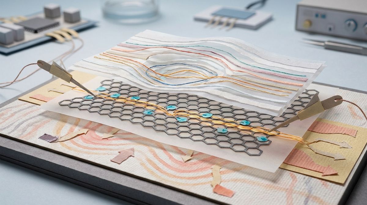
Imagine a world where the sensors in your smartphone, your car's autonomous driving system, and even the high-speed fiber optic cables under the ocean could all work significantly faster and with much higher precision. The bottleneck in these technologies often comes down to how we turn light into electricity. In the tiny, incredibly thin world of graphene, this process is governed by a race against time: how quickly an electron can capture energy from a photon before it loses that energy to heat. This breakthrough, brought to light by the collaborative efforts of Yishu Huang, Anand Nivedan, Florian Ludwig, Bohai Liu, Michiel Debaets, Steven Brems, Hai I. Wang, Alessandro Principi, Dries Van Thourhout, Christian Haffner, Aron W. Cummings, and Klaas-Jan Tielrooij, represents a significant leap in our ability to control this race, effectively engineering how electrons cool down to unlock unprecedented sensing capabilities.
At the heart of modern optoelectronics lies the photodetector, a device that translates light into electrical signals. Graphene has long been hailed as a superstar material for this task because of its unique electronic properties, including its extreme mobility and its ability to absorb light across a wide spectrum of wavelengths. However, graphene faces a fundamental physical hurdle known as the hot carrier problem. When a photon strikes a graphene sheet, it imparts energy to an electron, kicking it into a higher energy state. These excited electrons are referred to as hot carriers because they possess much more kinetic energy than the surrounding electrons in the material.
In a perfect world, these hot carriers would be swept through the device by an electric field to create a measurable current before they lose their energy. However, in reality, these electrons are in a frantic race against thermalization. They immediately begin to collide with other electrons and with the vibrations of the crystal lattice, known as phonons. These collisions act like friction, converting the useful electrical energy of the hot carriers into useless heat. This rapid cooling process happens on incredibly short timescales, often much faster than the time it takes for the device to register a useful signal. This results in a loss of responsivity, meaning the device becomes less sensitive to light, and a loss of signal strength, which limits the speed at which the device can operate.
The researchers realized that instead of simply trying to make graphene better, they could change the environment surrounding the graphene to control how the electrons cool. This is the concept of engineering hot carrier cooling dynamics. Think of it like a runner trying to maintain high speed on a track. If the track is a high-friction surface like sand, the runner loses energy almost instantly. If the track is smooth ice, they can maintain that high speed for much longer. In this research, the "track" is the interface between the graphene and the material underneath it.
By carefully selecting and designing the substrate—the material the graphene sits on—the scientists can manipulate the rate at which energy is transferred from the "hot" electrons in the graphene to the cooler atoms in the substrate. By slowing down this energy transfer, or "engineering the cooling," the researchers can extend the lifetime of the hot carriers. This gives the electrical signal more time to develop, effectively turning a weak, fleeting spark of energy into a robust, measurable electrical current. This ability to control the cooling rate is the fundamental key to making graphene-based sensors that are both faster and more sensitive than anything previously possible.
To understand how this works, we must dive into the interaction between electrons and phonons. In a solid-state device, energy transfer occurs through various scattering mechanisms. One of the most dominant is electron-phonon scattering, where an energetic electron bumps into a vibrating atom in the crystal lattice, transferring its kinetic energy to that atom. In a standard graphene device, these vibrations (phonons) can travel very easily into the underlying substrate, carrying the energy away from the graphene layer and into the bulk material, effectively cooling the electrons too quickly for optimal detection.
The experimental setup used in this research involves a carefully engineered interface. The researchers likely utilized specific dielectric materials or surface treatments to create a barrier or a specific type of vibrational environment. By modifying the surface of the substrate or the nature of the interface, they can alter the density and the type of phonons that interact with the graphene. For example, they might use a substrate that does not support certain types of high-energy vibrations, or they might create an interface that prevents energy from leaking away efficiently.
When a photon hits the graphene, it creates an electron-hole pair. Because the cooling process has been slowed down through this engineered interface, these carriers stay at a higher energy level for a longer duration. This extended lifetime means that the carriers have more time to travel through the material and contribute to the photocurrent. The charge carriers are essentially kept in a high-energy state long enough for the device's internal electric field to capture them, resulting in a higher electrical output for every photon that strikes the surface.
The study demonstrated that by controlling the cooling dynamics, the researchers could significantly influence the electrical performance of the photodetector. Specifically, they observed a direct correlation between the rate of carrier cooling and the device's responsivity. As they successfully engineered the environment to slow the cooling of the hot carriers, the responsivity of the detector improved. This confirms that the speed at which electrons lose their energy is not just a secondary side effect, but a primary factor that determines how well a graphene-based sensor performs.
Furthermore, the research provided insights into how the choice of substrate and the thickness of the interface layer affect the carrier lifetime. They were able to observe how different interfacial properties changed the energy relaxation rate of the carriers. This provides a mathematical and physical roadmap for designers to optimize photodetectors. Instead of relying on the natural, rapid cooling properties of graphene, engineers can now use these findings to "tune" the device, designing specific material stacks that provide the exact carrier lifetime needed for a particular application, whether that be ultra-fast communications or high-sensitivity light sensing.
This research is significant because it moves graphene technology from a phase of observation to a phase of active engineering. For years, the rapid cooling of carriers in graphene was seen as an inherent limitation that could not be easily overcome. This research flips that narrative, proving that the environment of the graphene is just as important as the graphene itself. By mastering the dynamics of hot carriers, we open the door to a new class of optoelectronic devices.
The implications for high-frequency communication are immense. As we move toward 6G and beyond, the demand for sensors that can respond to incredibly fast pulses of light is growing. Traditional silicon-based detectors are reaching their physical limits. Graphene, with its ability to be engineered at the atomic level, offers a path forward. Additionally, the ability to increase responsivity without increasing noise is critical for medical imaging and remote sensing, where detecting a single photon can be the difference between a successful diagnosis and a missed detection.
While these results are groundbreaking, there are several hurdles that remain before this technology can be deployed in your next smartphone. One major challenge is scalability. While it is possible to engineer a perfect interface in a controlled laboratory environment using advanced deposition techniques, replicating that exact same interface across a large-scale silicon wafer is an immense manufacturing challenge. The precision required to control carrier cooling at the atomic scale is extremely high, and maintaining that precision across millions of individual devices is a significant hurdle for industrial-scale production.
Furthermore, there is the issue of thermal management and stability. While slowing down the cooling of hot carriers is great for signal detection, it also means that the device might retain more heat. In a high-power application, this could lead to thermal instability or even damage to the device if the heat is not managed through other means. Additionally, the long-term stability of these engineered interfaces needs to be tested. We need to ensure that the delicate atomic arrangement that controls the carrier cooling doesn't degrade over time due to environmental exposure or repeated use. Finally, more work is needed to understand how these devices perform under a wider range of temperatures and light intensities to ensure they are robust enough for real-world use.
The ability to engineer hot carrier dynamics in graphene has a vast array of potential real-world applications. In the realm of telecommunications, this technology could lead to much faster optical receivers, enabling the next generation of ultra-high-speed internet and wireless communication systems. As data demands grow, the ability to process light-based signals with higher efficiency and speed will be essential for global connectivity.
In the field of autonomous transportation, LIDAR (Light Detection and Ranging) systems require extremely fast and precise light sensing to map surroundings in real-time. A more sensitive and faster graphene photodetector could allow autonomous vehicles to see further and react more quickly to obstacles. Furthermore, in medical diagnostics, highly sensitive photodetectors can be used in advanced imaging techniques, allowing for non-invasive, high-resolution scans that can detect diseases at their earliest stages. Finally, in the field of quantum technology, controlling individual charge carriers is a fundamental requirement, and this research provides a new method for managing electron energy at the quantum scale.
If you remember only one thing from this research, let it be this: the speed at which electrons lose their energy is the key to unlocking the true potential of graphene-based sensors, and we can now learn to control that speed by engineering the environment around the graphene.
Question: What exactly is a hot carrier in graphene?
Answer: When a photon hits an electron in graphene, it gives that electron a massive boost of kinetic energy. Because this electron now has much higher energy than the electrons around it, scientists call it a hot carrier. The goal in electronics is to use that energy to create a signal before the electron loses it.
Question: Why is graphene's rapid cooling a problem for sensors?
Answer: The problem is that electrons in graphene tend to lose their energy to heat very quickly through a process called thermalization. If the energy is lost too fast, the sensor doesn't have enough time to convert that light energy into an electrical signal, which makes the sensor less sensitive and less efficient.
Question: How can you "engineer" the cooling of an electron?
Answer: You can do this by changing the material that the graphene is sitting on. By choosing specific substrates or adding specific layers, you can change how easily vibrations (phonons) move away from the graphene. This allows you to essentially control how long the electron stays "hot" and useful.
Question: Is this technology ready for my phone right now?
Answer: Not quite yet. While the science is proven in a lab setting, it is still very difficult to manufacture these precisely engineered materials on a large scale. We still need to work on making the process reliable, affordable, and stable for mass production.
Question: What are the benefits of a better photodetector?
Answer: Better photodetectors mean faster internet, more accurate self-driving cars, better medical imaging, and more efficient sensors for everything from environmental monitoring to space exploration. It's about turning light into information more quickly and accurately.
The research conducted by Yishu Huang and the team of researchers marks a pivotal shift in the study of graphene-based optoelectronics. By moving away from viewing electron cooling as an inevitable loss and instead treating it as a variable that can be engineered, they have provided a new toolkit for the next generation of sensor technology. As we continue to master the interface between materials, the promise of graphene—to revolutionize how we interact with the world through light—becomes increasingly tangible. The transition from fundamental physics to practical engineering is well underway, and the results could redefine the speed of our digital future.
Serious about B2B integration? Test our premium Pulsed Electrical Resistive Carbon Heating turbostratic graphene in your lab. 100g sample packs available now.
Explore More
Researchers discover naturally formed graphene sheets and carbon ovals in stingless bee hives, creating a novel emergent material with powerful blue light...

Discover how rippled graphene pores act as fluidic memristors, enabling advanced synaptic functionalities for the next generation of neuromorphic computing.

Learn how to use electromechanical responses in gapped graphene to measure electronic temperature and band gaps using traveling flexural waves.