
Nature's Nanotech: Graphene and Blue Emission Found in Bee Hives
Researchers discover naturally formed graphene sheets and carbon ovals in stingless bee hives, creating a novel emergent material with powerful blue light...
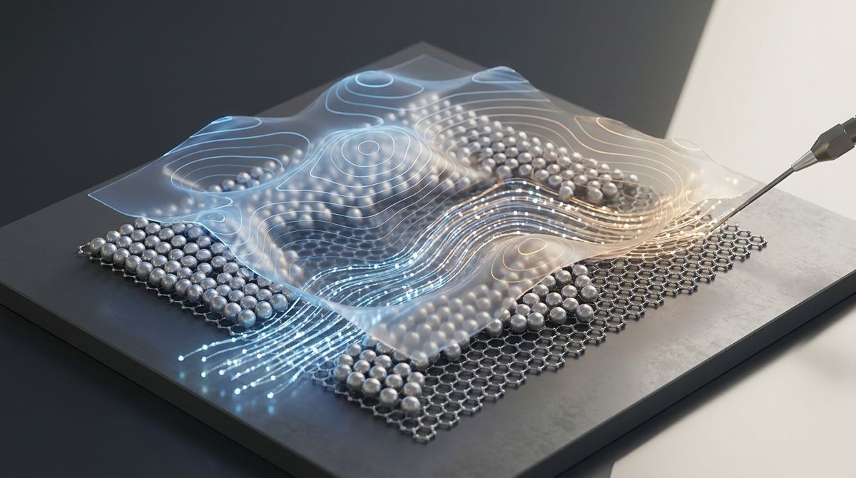
Imagine a world where the very materials making up our microchips can be tuned like a musical instrument, where their electrical properties shift precisely as they are layered. As electronic devices shrink toward the atomic scale, the way different materials touch each other becomes more important than the materials themselves. This research explores a frontier where we can control how electricity flows by manipulating the tiny, complex dance of atoms at the boundary between metal and carbon.
As the semiconductor industry pushes toward smaller and faster devices, engineers face a persistent obstacle known as contact resistance. When a metal wire is connected to a semiconductor, there is an inherent barrier that electrons must jump over, which generates heat and slows down the device. In traditional silicon-based electronics, this interface is often a bottleneck that limits how small a transistor can be and how much power it consumes. As we move into the era of two-dimensional materials, the problem changes from managing bulk materials to managing interfaces.
When you place a metal like silver on top of a material like graphene, the two do not simply sit together as separate entities. Instead, they interact in a way that can either help or hinder the flow of charge. If the atoms of the metal do not align well with the structure of the graphene, the resulting electronic "glitches" can lead to high resistance and unstable performance. Furthermore, the industry lacks a complete understanding of how these layers behave when they are only one or two atoms thick. Standard electrical models often fail when the interface becomes the dominant feature of the device, leaving engineers to guess how different metal-carbon combinations will perform in a real-world chip.
The core idea behind this research is that the electrical identity of a metal is not fixed if that metal is made extremely thin. Usually, we think of silver as a constant: it always conducts electricity in a very specific way. However, when silver is reduced to a two-dimensional layer and placed on graphene, its electronic properties become "phase-dependent." This means that the way silver behaves—how much energy it takes for an electron to move through it and how many electrons it can carry—depends entirely on the structural phase or the density of the silver atoms at that specific interface.
By using graphene as a specialized buffer between the silver and the silicon carbide substrate, scientists can create a playground where they can study these changes. Instead of seeing the metal as a static component, this research suggests we should view the interface as a tunable component. If we can control the phase of the silver layer, we can effectively design the electronic structure of the contact, allowing us to engineer electrical properties that would be impossible with bulk metals.
To understand this system, we must look at the three distinct layers involved: the silicon carbide substrate, the graphene layer, and the silver layer. The process begins with silicon carbide, which acts as the rigid foundation. Through a process of high-temperature heating, silicon atoms are evaporated from the surface, leaving behind a perfectly arranged, single-layer sheet of carbon atoms known as graphene. This graphene layer is not just a passive surface; it acts as an atomically smooth, highly conductive template that dictates how the next layer will behave.
When silver is deposited onto this graphene-on-SiC platform, a complex interaction begins. The silver atoms attempt to find a stable position on the hexagonal lattice of the graphene. Because graphene is a two-dimensional material, the silver atoms are highly sensitive to the environment provided by the carbon atoms. This creates a phenomenon known as electronic coupling. The electrons in the silver layer and the electrons in the graphene layer begin to interact, sharing energy and momentum. This interaction is what defines the electronic structure.
The researchers, including Sawani Datta, Boyang Zheng, Arpit Jain, Kathrin Küster, Joshua A. Robinson, Vincent H. Crespi, and Ulrich Starke, focused on how this interaction changes as more silver is added. As the coverage of silver increases, the atoms move from being isolated individuals to forming small clusters, and eventually, they coalesce into a continuous, two-dimensional film. Each of these stages represents a different structural phase, and each phase presents a unique electronic fingerprint to the electrons trying to pass through the junction.
The research revealed that the electronic structure of the silver layer is highly sensitive to its coverage and structural phase. As the silver layer transitions through different stages of density and arrangement, the density of states—which is essentially the number of available "seats" for electrons to occupy—undergoes significant shifts. This is not a smooth, linear change but rather a series of shifts that depend on the specific arrangement of the silver atoms on the graphene lattice.
One of the most critical findings is how the presence of the graphene layer modifies the silver's behavior. The research showed that the electronic states of the silver are not just resting on top of the graphene; they are hybridized with it. This means the silver's electrons and the graphene's electrons become somewhat intertwined. This hybridization is phase-dependent, meaning that as the silver layer changes its physical structure, the way its electrons mix with the graphene's electrons also changes. This effect is what ultimately determines the electrical conductivity and the energy barriers that electrons face when moving through the interface.
Furthermore, the study highlighted that the silver layer does not behave like a bulk metal even when it starts to form a continuous sheet. Because the interface with the graphene is so dominant, the two-dimensional nature of the silver layer imposes its own rules. The electronic structure is a direct consequence of the competition between the silver-silver atomic bonds and the silver-graphene interaction. Understanding this competition is the key to predicting how these nano-scale contacts will function in actual electronic circuits.
This research is significant because it provides a blueprint for interface engineering at the atomic scale. For decades, the semiconductor industry has relied on bulk properties to predict how materials will behave. However, as we move toward "More than Moore" technologies—where devices are integrated using novel materials like graphene and 2D metals—those bulk rules no longer apply. We need to know how to design the interface itself to achieve specific goals, such as reducing resistance or managing charge injection.
By proving that the electronic structure is phase-dependent, the researchers have shown that we have a new "knob" to turn in device design. If an engineer needs a contact with a specific electrical characteristic, they may not need to find a whole new material; they might only need to control the thickness or the deposition conditions of a metal like silver to reach the desired electronic phase. This capability could lead to much more efficient power electronics, faster high-frequency communication components, and more stable sensors.
While these findings are groundbreaking, it is important to distinguish between fundamental scientific discovery and commercially ready technology. This research was conducted in a highly controlled laboratory environment using silicon carbide substrates, which are significantly more expensive and difficult to manufacture than the standard silicon wafers used in mass-market electronics. The ability to grow these perfect, single-layer graphene sheets on large-scale wafers remains a major industrial challenge.
Additionally, while the phase-dependent electronic structure offers exciting possibilities for tuning, it also introduces complexity. Controlling the exact thickness and phase of a metal layer across an entire microchip with atomic precision is an immense engineering hurdle. There are also questions regarding the long-term stability of these thin silver layers. In a real-world device, silver can migrate or oxidize over time, which would change its phase and destroy the carefully engineered electronic structure that was intended to improve performance. Further research is needed to ensure these interfaces remain stable under the heat and electrical stress of everyday operation.
The implications for real-world technology are vast, particularly in the field of high-speed electronics. As we move toward 6G communications and ultra-fast computing, we need interconnects and contacts that can handle incredibly high frequencies without losing signal to resistance. The ability to engineer the electronic structure of silver-graphene interfaces could lead to a new generation of ultra-low-resistance interconnects that allow chips to run faster while consuming less power.
Another promising area is in the development of flexible and wearable electronics. Graphene is famously flexible, and if we can master the deposition of thin, stable metal layers on graphene, we can create circuits that can be bent or stretched without losing their electrical properties. Furthermore, the sensitivity of these interfaces to their environment makes them potential candidates for high-precision chemical and biological sensors, where the change in a metal's phase or electronic state could be used to detect the presence of specific molecules.
If there is one takeaway from this study, it is that the interface is no longer just a boundary between two materials; it is a functional, tunable component of the device itself.
What is the significance of graphene in this research?
Graphene acts as a highly conductive and atomically smooth template that allows scientists to study how metals behave at the most fundamental level. It provides a unique surface that interacts with the metal atoms, allowing for the creation of a unique electronic environment that does not exist in traditional bulk materials.
Why did the researchers choose silver for this study?
Silver is one of the best conductors of electricity known to science. By studying silver at the two-dimensional limit, researchers can explore the absolute limits of how much conductivity can be achieved at the nanoscale, which is essential for the future of microelectronics.
What does "phase-dependent" actually mean in this context?
In this context, it means that the electrical properties of the silver change based on how the atoms are arranged. As the silver goes from being individual atoms to small clusters and finally to a continuous sheet, its electronic structure shifts, meaning its electrical behavior changes depending on its physical state or "phase."
Will this research lead to cheaper computer chips immediately?
No, because the research is currently focused on fundamental physics and laboratory-scale materials like silicon carbide. While it provides the knowledge needed to design better chips, the industrial processes required to manufacture these complex interfaces on a mass scale are still being developed.
How does the graphene-silver interface help reduce heat in electronics?
Heat in electronic devices is often caused by resistance at the junctions where different materials meet. By using graphene to create a more efficient, engineered interface, we can reduce the energy lost as heat, leading to cooler and more efficient devices.
The study of the phase-dependent electronic structure of silver on graphene-silicon carbide interfaces marks a significant step forward in our ability to control matter at the atomic level. By moving beyond the limitations of bulk material properties and embracing the complexity of two-dimensional interfaces, researchers like Sawani Datta and Ulrich Starke are opening new doors for the future of semiconductor technology. While engineering challenges remain in scaling these findings for mass production, the ability to tune the electronic identity of a metal through interface engineering provides a powerful new tool for the next generation of electronic innovation.
Serious about B2B integration? Test our premium Pulsed Electrical Resistive Carbon Heating turbostratic graphene in your lab. 100g sample packs available now.
Explore More
Researchers discover naturally formed graphene sheets and carbon ovals in stingless bee hives, creating a novel emergent material with powerful blue light...

Discover how rippled graphene pores act as fluidic memristors, enabling advanced synaptic functionalities for the next generation of neuromorphic computing.

Learn how to use electromechanical responses in gapped graphene to measure electronic temperature and band gaps using traveling flexural waves.