
Unlocking Quasicrystal Physics in 30-Degree Twisted Bilayer Graphene
Research on 30° quasi-periodic twisted bilayer graphene reveals a unique, fractal-like energy structure under magnetic fields, paving the way for novel...
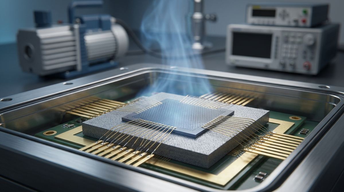
Nitrogen Oxide (NO) is a highly toxic gas found in industrial emissions and urban smog. Detecting it at low concentrations is critical for environmental monitoring and workplace safety. While pristine graphene is often the starting point for many nano-electronics, it frequently lacks the chemical reactivity required for high-sensitivity gas detection.
Recent research (Yadav et al., 2025) has demonstrated that modifying the graphene lattice can fundamentally change its sensing capabilities. Specifically, the study found that introducing a single vacancy (SV) defect—a missing carbon atom in the hexagonal lattice—dramatically increases the adsorption energy and sensitivity for NO gas. While metal doping (using Copper, Gold, or Platinum) provides moderate improvements, the defected graphene structure outperformed both pristine and doped versions, achieving a sensitivity of 51.1 percent.
For an engineer or a small lab, this suggests a shift in strategy: instead of focusing on expensive metal-doping processes, the priority should be on controlled defect engineering to create high-performance, low-cost gas sensors.
To build a prototype based on these findings, you will need the following components. Note that the research was conducted using Quantum ATK (a simulation tool), so these requirements represent the physical implementation of those theoretical models.
1. Graphene Substrate: High-quality CVD-grown graphene transferred onto a silicon/silicon dioxide (Si/SiO2) substrate.
2. Electrodes: Gold (Au) or Palladium (Pd) for contact pads, typically deposited via electron-beam evaporation or sputtering.
3. Defect Induction Tool: An Argon plasma cleaner or a Focused Ion Beam (FIB) system for creating controlled vacancies.
4. Gas Delivery System: A mass flow controller (MFC) and a certified Nitrogen Oxide (NO) gas cylinder.
5. Measurement Electronics: A high-precision Source Measure Unit (SMU) capable of measuring nano-ampere current changes.
6. Environmental Chamber: A small, sealed glass or stainless steel chamber to control gas concentration and humidity.
Building a functional sensor requires precise control over the graphene surface. Follow these steps to move from a raw sheet to a sensing device.
1. Substrate Preparation: Clean your Si/SiO2 substrate using a standard Piranha etch or an acetone/isopropanol (IPA) rinse to ensure no organic contaminants remain.
2. Graphene Transfer: Use a standard PMMA-assisted transfer method to place the CVD graphene onto the substrate. Ensure the graphene is continuous and free of wrinkles or polymer residue.
3. Electrode Patterning: Use photolithography to define electrode patterns. Deposit your metal contacts (e.g., 5nm Ti for adhesion and 50nm Au for conductivity). This creates a two-terminal or four-terminal device configuration.
4. Defect Engineering: This is the most critical step. To replicate the research findings, you must introduce vacancies.
- For small-scale lab testing: Use a low-power Argon plasma etch. You must carefully calibrate the power (typically <10W) and exposure time (seconds) to avoid destroying the entire graphene sheet.
- For high-precision prototyping: Use a Focused Ion Beam (FIB) to target specific areas, though this is significantly more expensive and slower.
- Engineering Assumption: Since the research focuses on a single vacancy, a practical engineer should aim for a controlled defect density rather than a single atom. Aim for a low density of vacancies to maintain the structural integrity of the sheet.
5. Encapsulation and Connection: Wire-bond the gold pads to your measurement setup. Ensure the sensor is placed in a way that allows gas to flow directly over the active graphene area.
To validate that your sensor is performing according to the theoretical sensitivity of 51.1 percent, follow this testing protocol.
1. Baseline Resistance Measurement: Place the sensor in a controlled environment (pure Nitrogen or dry air). Measure the baseline resistance (R0) and the baseline I-V (current-voltage) characteristics.
2. Gas Exposure Cycles: Introduce NO gas at varying concentrations.
- Proposed starting range: 1 ppm to 50 ppm.
- The research does not specify the exact concentration for the 51.1 percent sensitivity, but for industrial safety, the 1-10 ppm range is a standard starting point.
3. Sensitivity Calculation: Calculate the sensitivity (S) using the formula:
S = [(R_gas - R_air) / R_air] 100
Where R_gas is the resistance in the presence of NO and R_air is the resistance in baseline air.
4. Recovery and Response Time: Monitor how long it takes for the resistance to return to baseline after the gas flow is stopped. This is vital for determining if the sensor is reusable.
5. Selectivity Testing: Test the sensor against interfering gases such as CO, CO2, or humidity (H2O). This determines if the defects are specifically reacting with NO or just any gas that hits them.
While the research provides a clear roadmap, several practical hurdles must be addressed during implementation.
1. Adsorption Energy and Reversibility: The study reports a very high adsorption energy of 8.316 eV for the defected graphene. In engineering terms, this is a double-edged sword. While high adsorption energy means high sensitivity, it also means the NO gas may bond so strongly to the vacancy that it cannot be removed easily.
- Risk: The sensor may be "one-way," meaning it works once and then requires high heat (thermal regeneration) to clear the surface.
- Mitigation: Plan for an integrated micro-heater on the substrate to periodically bake the sensor to reset it.
2. Defect Density Control: It is extremely difficult to control the exact number of vacancies. Too few defects, and the sensitivity will be low. Too many defects, and the graphene sheet will lose its electrical conductivity or suffer mechanical failure.
- Risk: Inconsistent sensor performance across different batches.
- Mitigation: Use Raman spectroscopy to characterize the D-peak (defect peak) to quantify the defect density before and after the etching process.
3. Environmental Interference: Real-world humidity can drastically change the electrical characteristics of graphene.
- Risk: False positives caused by moisture rather than NO.
- Mitigation: Include a humidity sensor in your device to allow for software-based compensation of the data.
This guide is based on the computational findings of Yadav, Philip, and SanthiBhushan (2025). The core engineering takeaway is that for Nitrogen Oxide detection, the structural defects (vacancies) are more effective than chemical doping with transition metals. While the research was performed using the Quantum ATK simulation framework, the transition to physical prototyping requires careful management of plasma etching and thermal regeneration to handle the high adsorption energy identified in the study.
Serious about B2B integration? Test our premium Pulsed Electrical Resistive Carbon Heating turbostratic graphene in your lab. 100g sample packs available now.
Explore More
Research on 30° quasi-periodic twisted bilayer graphene reveals a unique, fractal-like energy structure under magnetic fields, paving the way for novel...

Researchers discover naturally formed graphene sheets and carbon ovals in stingless bee hives, creating a novel emergent material with powerful blue light...

Discover how rippled graphene pores act as fluidic memristors, enabling advanced synaptic functionalities for the next generation of neuromorphic computing.