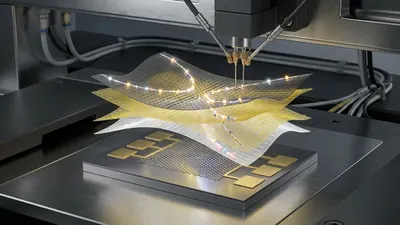
Angle-Resolved Berry Curvature Using the Nonlinear Hall Effect
Researchers develop a new technique using the nonlinear Hall effect in ballistic graphene to create high-resolution maps of Berry curvature, a key quantum...
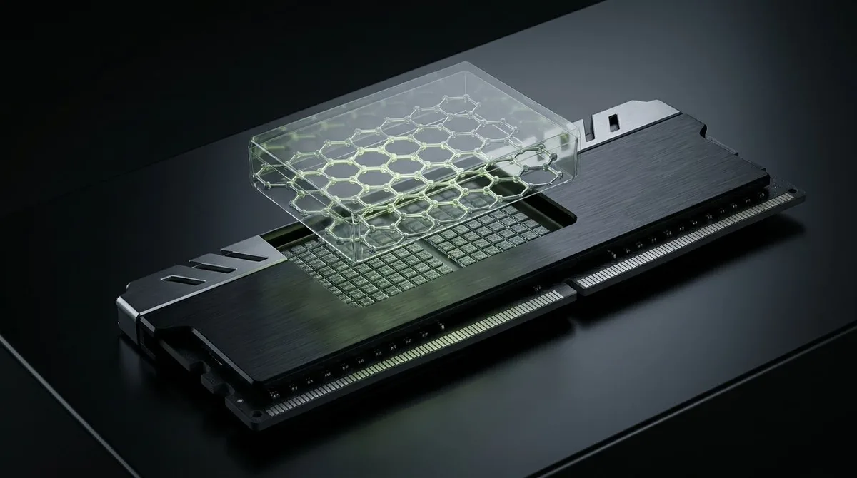
Graphene in PC memory is a credible research direction, but the phrase can hide several very different technologies. A memory cell that includes graphene is not automatically a replacement for the RAM in a desktop computer. It may instead be a prototype nonvolatile storage device, an electrode inside a layered transistor, or a component intended for an entirely different computing architecture. The useful question is which memory function the material performs, and what has actually been demonstrated.
For PC users, the distinction matters. A computer needs fast temporary working memory, persistent storage, and small caches close to its processor. These components solve different problems. A material improvement in one part of that hierarchy does not transfer automatically to the others. Graphene becomes interesting when its thinness, electrical properties, or interfaces improve a particular device mechanism. The engineering case must then survive comparison with the complete memory system that a real computer requires.
DRAM provides the main working memory used by running programs. Its stored information needs refreshing, and ordinary DRAM loses its contents when power is removed. SRAM, commonly used in processor caches, also stores information only while powered, but uses a different circuit structure. Flash memory retains information without continuous power and supports persistent storage, including the NAND flash inside solid-state drives.
These categories establish different priorities. Main memory must handle frequent reads and writes with predictable latency. A cache must fit tightly into a processor’s timing and power constraints. Storage emphasizes capacity, persistence, reliability, and cost as well as performance. A candidate technology can excel at retaining charge and still be unsuitable for an intensely rewritten cache. It can also demonstrate an impressive programming pulse without delivering the sustained bandwidth of a finished SSD.
When evaluating graphene electronics research, therefore, begin with the target. Ask whether a study measures a transistor, a memory cell, an array, or a complete chip. Then ask whether its claimed advantage concerns programming, erasing, reading, retention, endurance, or total system energy. Those measurements should not be treated as interchangeable.
In a floating-gate memory, stored electrical charge changes the behavior of a transistor. The reading circuit detects that change and interprets it as information. A sufficiently insulating barrier helps keep the charge in place when the power is off. Graphene can act as a thin charge-storage layer in some designs. In others, it forms the conducting channel through which the stored state is sensed. Its role depends on the complete stack, not simply on whether carbon appears somewhere in the device.
The surrounding materials are equally important. A tunneling barrier must permit useful programming while limiting unwanted leakage. Interfaces must remain consistent across cells. Contacts must deliver current without overwhelming the benefit of the active material. The device also needs an operating window that can distinguish stored states despite manufacturing variation and temperature changes. Graphene’s presence alone does not establish that these requirements have been met.
An early example is the 2011 graphene flash memory work described by IBM Research. The researchers integrated large-area graphene grown by chemical vapor deposition into a floating-gate structure. Their reported device behavior and scaling simulations supported further investigation of graphene as a charge-storage material. This was a research demonstration, rather than evidence that a consumer computer could accept a graphene RAM upgrade.
A stronger recent example is the 2025 Nature paper Subnanosecond flash memory enabled by 2D-enhanced hot-carrier injection. The authors reported a graphene-channel flash device programmed with a 400-picosecond pulse and endurance exceeding 5.5 million cycles under their experimental conditions. The proposed mechanism uses the thin channel to improve the electrical conditions for carrier injection.
The result is significant because programming speed is a major constraint for nonvolatile memory. However, a programming pulse is not the same measurement as a processor’s completed memory access. A working system must also select a cell, provide appropriate voltages, read or verify its state, move data, and handle errors. The paper’s device result cannot by itself establish the latency, capacity, or power consumption of a future PC memory module.
For the same reason, it would be misleading to turn this result into an unconditional claim that graphene makes a computer faster. Application performance depends on the processor, software, workload, interconnects, and memory controller. The responsible interpretation is narrower: this experiment establishes an unusually fast programming mechanism worth developing and testing at larger scales.
Another 2025 Nature study, A full-featured 2D flash chip enabled by system integration, demonstrated a 1-kilobit NOR flash module integrated with CMOS support circuitry. Its memory cells used monolayer molybdenum disulfide and a hafnium-oxide/platinum stack. It should not be relabeled as a graphene memory chip merely because both studies belong to the broader field of two-dimensional electronics.
The distinction is instructive. The integrated chip included instruction handling and peripheral circuitry, and was tested using a 5-MHz clock. Its reported cell-level performance and system implementation answer different questions from a standalone ultrafast device experiment. Together, these studies illustrate why the path from promising materials to useful memory requires several kinds of evidence, rather than one headline number.
The practical lesson for engineers is to examine the entire chain. A fast cell must become a repeatable array. The array must connect to drivers and sensing circuits. The resulting chip must operate through an interface that a host system can use. Each step can introduce delays, energy costs, and reliability constraints absent from the original experiment.
A useful qualification program would test more than the fastest operating point. Retention should be evaluated under specified temperatures and aging conditions. Endurance should include the consequences of repeated programming and erasing. Researchers should disclose how many cells were tested, how their behavior varied, and what operating voltages were required. Claims about scalability need evidence that the fabrication process can produce useful arrays consistently.
System engineers would also need to characterize read disturbances, failed writes, and the recovery behavior after interrupted power. These are not minor details for memory containing a user’s files or an operating system’s active state. A controller may correct some errors, but that controller adds complexity and overhead. Its effect belongs in any comparison with established technology.
Manufacturing presents another set of questions. A high-quality small sample does not establish wafer-scale uniformity. Transferring a film can introduce contamination or damage. Processing the surrounding stack can alter material properties. Packaging can impose mechanical and thermal stress. An attractive device design must be compatible with a repeatable process and an economically realistic test strategy.
Memory research often involves carefully controlled films and interfaces. The relevant specifications can include layer count, continuity, defects, contamination, contact resistance, and the condition of a tunneling barrier. These are different requirements from those used to qualify an additive for a coating, composite, or concrete mixture.
That difference matters when discussing commercial graphene applications. A successful formulation using dispersed flakes does not prove that the same material can be placed directly into a semiconductor memory stack. Conversely, a tiny memory device does not establish a demand forecast for industrial graphene powder. Material form and device function should remain explicit throughout the discussion.
For suppliers and customers, a sensible first step is to define the actual material interface before discussing volumes or performance promises. Specify the deposition or transfer process, acceptable contamination, substrate, electrical measurements, and downstream fabrication conditions. Without that information, the word graphene is too broad to support a useful technical comparison.
A claim about a PC product should identify a product and its intended use. Useful evidence would include a manufacturer’s specification, a supported interface, capacity, operating conditions, reliability information, and independent system testing. A statement that a product contains graphene should also explain whether the material participates in memory storage or only in packaging or thermal management.
The studies discussed here do not demonstrate a retail replacement for a standard PC RAM module. They demonstrate specific research devices and an important, separate 2D integration approach. That leaves substantial room for innovation without requiring an invented launch date or a promise that current memory products are about to disappear.
An informed reader can track progress by watching for larger arrays, stronger distributions of measured results, validated controller behavior, and realistic application benchmarks. A clear demonstration of the targeted function is more useful than a comparison built from incompatible measurements. The most persuasive future milestone would connect an identified materials advantage to a reproducible improvement in a complete system.
Graphene-based nonvolatile research devices can retain stored information, but that does not establish a compatible persistent replacement for ordinary DRAM. Such a replacement would need the required capacity, endurance, interface behavior, and system support. Persistence also changes how software and security mechanisms handle information after shutdown.
No. It measures a particular device programming operation. A finished drive must manage arrays, controllers, data transfer, error correction, and repeated workloads. Those components determine the performance users actually observe. Device speed is one input to that engineering problem.
No. Two-dimensional materials include different conductors, semiconductors, and insulators. The integrated NOR chip described above used a molybdenum disulfide channel. Naming the actual materials prevents unrelated results from being combined into a misleading commercialization story.
Graphene offers credible ways to investigate thinner charge-storage structures and faster nonvolatile programming. The clearest opportunity is to improve a defined memory function and then demonstrate that improvement at array and system scales. For PC buyers, these papers are evidence of a research direction, rather than a purchasing specification. For researchers and engineers, they provide concrete mechanisms and integration challenges to test next.
Serious about B2B integration? Test our premium Pulsed Electrical Resistive Carbon Heating turbostratic graphene in your lab. 100g sample packs available now.
Explore More
Researchers develop a new technique using the nonlinear Hall effect in ballistic graphene to create high-resolution maps of Berry curvature, a key quantum...
Explore how alternating-twist multilayer graphene's unique response to in-plane magnetic fields, as modeled by new research, opens doors to advanced...
Research into graphene magnonics explores how topological frustration can create robust, one-way channels for spin waves, paving the way for future...