In-plane magnetic response and Maki parameter of alternating-twist multilayers
Explore how alternating-twist multilayer graphene's unique response to in-plane magnetic fields, as modeled by new research, opens doors to advanced...
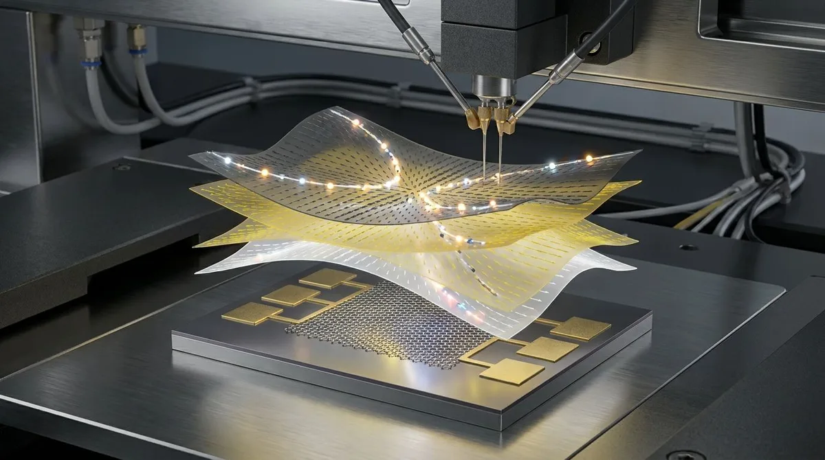
Imagine trying to navigate a complex city using only a compass. It tells you which way is north, but it gives you no information about the one-way streets, roundabouts, or hidden tunnels that truly govern the flow of traffic. For decades, physicists studying the movement of electrons in advanced materials have faced a similar problem. They understand the basic forces at play, but a deeper, more subtle set of "traffic rules" has remained difficult to map out in detail. These rules are governed by a quantum mechanical property called Berry curvature, an intrinsic feature of a material's electronic structure that acts like a hidden landscape of hills and valleys, guiding electrons on curved paths. A new study proposes a powerful method to finally create a detailed, high-resolution map of this hidden landscape.
The ability to control electron flow is the foundation of all modern electronics. In conventional materials like silicon, this is straightforward. But in the realm of quantum materials—a class that includes graphene, topological insulators, and Weyl semimetals—electrons behave in far more exotic ways. Their movement is influenced not just by electric and magnetic fields, but also by the intrinsic quantum geometry of the material itself. This geometry is described by the Berry curvature, which can be thought of as a kind of internal, momentum-dependent magnetic field that the material generates on its own. This property is responsible for a host of fascinating phenomena, including the anomalous Hall effect, which is crucial for spintronics and magnetic memory.
The central problem has been measuring this Berry curvature directly and with sufficient detail. Existing methods are often indirect, require complex experimental setups with powerful external magnetic fields, or can only measure an averaged, smeared-out value. They provide the "compass" but not the detailed street map. This lack of a precise measurement tool has been a major bottleneck, hindering our ability to fully understand, verify, and engineer new quantum materials for next-generation devices. The work from researchers Louis Primeau, Qiong Ma, and Yang Zhang introduces a novel technique to overcome this longstanding challenge, offering a way to chart this quantum terrain with unprecedented clarity.
The researchers' core idea is to use two key concepts: ballistic electrons and the nonlinear Hall effect. First, imagine an electron moving through a material. Usually, it’s constantly bumping into atomic lattice vibrations and impurities, scattering like a pinball. This is called diffusive transport. However, in an ultra-clean material over very short distances, an electron can travel without scattering at all, like a bullet fired in a vacuum. This is known as ballistic transport. High-quality graphene is an exceptional platform for observing this behavior due to its pristine atomic structure and high electron mobility.
Second is the Hall effect. The classic Hall effect occurs when you pass a current through a conductor and apply a magnetic field perpendicular to it. The magnetic force pushes the electrons sideways, creating a measurable voltage in the transverse direction. The researchers, however, focus on a more subtle version called the nonlinear Hall effect. This effect generates a similar transverse voltage but does so *without any external magnetic field*. Instead, the voltage arises from the material's intrinsic Berry curvature. It is "nonlinear" because this voltage is not proportional to the applied current, but rather to the square of the current, a unique signature that allows it to be isolated from other signals.
By combining these ideas, the team proposed a new measurement scheme. In a ballistic device, where electrons travel in straight lines, they can control the direction of that travel. By measuring the tiny nonlinear Hall voltage that appears, they can directly probe the Berry curvature that corresponds to that specific direction of electron momentum. By systematically changing the direction of the ballistic electron current, they can, point by point, build a complete, angle-resolved map of the Berry curvature. They have essentially created a "quantum protractor" to survey the material's internal geometric landscape.
While the paper details a general theoretical method, a material like single-crystal graphene is the ideal candidate for its experimental realization. The proposed system would begin with an impeccably clean sheet of graphene, a material whose two-dimensional nature and robust electronic properties make it a perfect laboratory for studying electron dynamics. This sheet would be carefully patterned into a specific geometry, such as a Hall bar with multiple terminals. This fabrication would likely be done using advanced nanolithography techniques. The quality of the material is paramount; any defects or impurities could cause electrons to scatter, destroying the ballistic transport needed for the measurement. This highlights the critical need for industrial-scale synthesis of high-purity materials, such as those produced by advanced graphene production machinery.
In the experiment, a current is injected into the graphene device. The device's geometry is designed to collimate the electrons, forcing them to travel ballistically in a specific, well-defined direction. As these electrons travel, the material's intrinsic Berry curvature exerts a subtle sideways force on them, causing them to deflect. This deflection leads to a small buildup of charge on one side of the device, creating a transverse voltage. This is the nonlinear Hall voltage.
The key is that this voltage is directly proportional to a quantity known as the Berry curvature dipole, which describes the distribution of the Berry curvature in momentum space. Crucially, the magnitude and sign of this voltage depend on the direction of the initial electron current relative to the crystal's axes. By rotating the device or reconfiguring the current paths, the researchers can measure this voltage for many different angles. Sophisticated electronics are used to isolate the tiny nonlinear signal, which scales with the square of the applied electric field, from the much larger linear background signals. By plotting the measured voltage as a function of angle, a detailed map of the Berry curvature is constructed.
The theoretical results presented in the paper demonstrate that this technique is not only feasible but also remarkably powerful. The authors' calculations show a clear, direct relationship between the angular dependence of the nonlinear Hall voltage and the underlying structure of the Berry curvature. Their model predicts that for a given material, the resulting angular plot of the voltage would act as a unique fingerprint of its electronic topology. They showed how this fingerprint reveals features that would be completely invisible to conventional, angle-averaged measurement techniques.
For instance, their model illustrated how the technique could distinguish between different types of topological materials, identifying the precise locations in momentum space where the Berry curvature is strongest. These "hot spots" are regions of intense quantum geometric effects and are of primary interest for designing new electronic functions. The research effectively provides a recipe for experimentalists: measure the nonlinear Hall response at various angles, and you will have a direct image of the Berry curvature landscape. This transforms Berry curvature from a theoretical abstraction into a tangible, measurable, and ultimately, an engineerable quantity.
This work represents a significant leap forward in the field of quantum materials metrology. Having a tool to precisely map Berry curvature is like an astronomer getting a new telescope with vastly improved resolution; suddenly, details of distant galaxies that were once blurry smudges become sharp, distinct structures. For materials scientists, this technique provides a powerful diagnostic tool to guide the discovery and synthesis of new materials. They can now get direct experimental feedback to verify and refine their theoretical models, dramatically accelerating the design-build-test cycle for advanced graphene electronics.
Furthermore, understanding the distribution of Berry curvature is essential for harnessing quantum phenomena for practical technology. Many proposed next-generation devices, from ultra-low-power transistors to fault-tolerant quantum computers, rely on engineering materials with specific topological properties. For example, materials with a large Berry curvature dipole are candidates for efficient charge-to-spin conversion, a key process for spintronic devices. Without a way to measure this property accurately, designing such materials has been a matter of trial and error. This new method provides the blueprint, enabling a more rational, engineering-driven approach to creating materials with tailored quantum functionalities.
It is important to recognize the practical challenges that lie ahead. The proposed technique relies on ballistic transport, which is a delicate state. It requires extremely high-quality, single-crystal materials and typically necessitates cryogenic temperatures to minimize thermal vibrations that can scatter electrons. This makes the experimental setup complex and currently limits the method to a laboratory setting. Scaling this up for industrial quality control on large-area materials, like commercial turbostratic graphene flakes, would be a formidable challenge.
The paper presents a theoretical framework and proof of principle. The next crucial step is rigorous experimental verification across a range of different materials. Scientists will need to test this method on known materials to confirm its accuracy and then apply it to novel quantum materials where the Berry curvature is unknown. Researchers will also need to investigate the effects of sample boundaries, contact configurations, and residual disorder on the accuracy of the measurements. Overcoming these hurdles will be essential to transition this technique from a specialized physics experiment into a standard characterization tool for materials science.
While direct commercial products based on this measurement technique itself are far off, its indirect impact could be enormous. By accelerating the fundamental understanding of quantum materials, this research paves the way for future breakthroughs in several key areas. In electronics, it could lead to the design of new types of transistors that exploit the anomalous velocity of electrons, potentially leading to faster and more energy-efficient computing.
In the field of spintronics, where information is encoded in an electron's spin, this technique could help identify materials ideal for generating and detecting spin currents without magnetic fields. This is a critical step toward creating spin-based memory and logic devices that are denser and less power-hungry than their charge-based counterparts. The insights gained could also be relevant for developing novel sensors, thermoelectric devices for waste heat recovery, and even catalysts, where the electronic surface states play a critical role. The ability to map Berry curvature provides a new knob for scientists to turn as they engineer materials for a wide spectrum of graphene applications.
If you take away just one thing from this research, let it be this: scientists have devised a new kind of high-resolution "quantum GPS" for electrons. By measuring a subtle nonlinear electrical effect in ultra-pure materials, they can now create detailed maps of the hidden geometric landscape that governs electron flow, opening a new door for designing the quantum materials that will power future technologies.
What is Berry curvature in simple terms?
Think of Berry curvature as an invisible landscape of hills and valleys that exists within a material's electronic structure. As an electron moves, this landscape gently nudges it, causing its path to curve even without an external magnetic field. This research provides a way to map the precise shape of that landscape.
Why are "ballistic electrons" important for this measurement?
Ballistic electrons travel without scattering off imperfections. This is crucial because it means their final trajectory is determined purely by the intrinsic Berry curvature of the material, not by random collisions. This provides a clean, unambiguous signal that can be used to map the curvature.
What is the difference between the normal Hall effect and the nonlinear Hall effect?
The normal Hall effect requires an external magnetic field to generate a transverse voltage and the voltage is directly proportional to the current. The nonlinear Hall effect requires no external magnetic field; the transverse voltage arises from the material's internal Berry curvature and is proportional to the square of the current.
Is this technology ready for commercial products?
No, not directly. This is a fundamental research tool for characterizing materials at a deep quantum level. Its value lies in enabling scientists and engineers to discover and design better materials, which will then be used in future commercial products, rather than being a commercial product itself.
How does this research relate to graphene?
Graphene's exceptionally clean atomic lattice and high electron mobility make it one of the best known platforms for achieving ballistic electron transport, especially at the nanoscale. It serves as a perfect, model system for demonstrating and perfecting this new measurement technique before applying it to more complex quantum materials.
The work by Louis Primeau, Qiong Ma, and Yang Zhang offers a powerful and elegant solution to a long-standing problem in condensed matter physics. By cleverly combining the physics of ballistic transport with the subtle signature of the nonlinear Hall effect, they have forged a new tool for exploring the quantum world. This angle-resolved technique effectively elevates Berry curvature from a fascinating theoretical concept to a precisely measurable and engineerable property. In doing so, it provides the missing map needed to navigate the complex terrain of quantum materials, accelerating our journey toward a new generation of electronics, spintronics, and quantum computing technologies.
Serious about B2B integration? Test our premium Pulsed Electrical Resistive Carbon Heating turbostratic graphene in your lab. 100g sample packs available now.
Explore More
Explore how alternating-twist multilayer graphene's unique response to in-plane magnetic fields, as modeled by new research, opens doors to advanced...
Research into graphene magnonics explores how topological frustration can create robust, one-way channels for spin waves, paving the way for future...
Discover how longitudinal nonreciprocal charge transport could revolutionize electronics by enabling one-way current flow in graphene without magnetic fields.