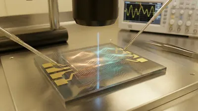
Gate-Tunable Antiferromagnetism in Graphene Heterostructures for Spintronics
Researchers demonstrate a novel method for creating gate-tunable synthetic antiferromagnetism in a graphene-based heterostructure, paving the way for new...
The device you are reading this on is a marvel of engineering, but it has a fundamental weakness: heat. Every calculation performed by its tiny processors generates waste heat, and this heat is the enemy of performance and longevity. As we push electronics to become smaller, faster, and more powerful, we are hitting a thermal wall where our current silicon-based technology can no longer keep up. The search for a new class of materials that can operate more efficiently and withstand higher temperatures is one of the most critical quests in modern electronics. A promising new study demonstrates how combining two different atom-thin materials, graphene and molybdenum disulfide, can create a transistor that not only runs better but also stays remarkably stable when things get hot.
For decades, the silicon field-effect transistor (FET) has been the undisputed workhorse of the digital world. But as we shrink these transistors to the nanometer scale, we encounter a host of problems. Quantum mechanical effects begin to interfere with their operation, and the electrical contacts needed to get signals into and out of the tiny silicon channel become a major source of performance-killing resistance and heat. To move forward, scientists are exploring alternatives to silicon, with a family of materials known as transition metal dichalcogenides, or TMDs, emerging as a leading candidate. Molybdenum disulfide (MoS2) is one of the most studied TMDs; it is a natural semiconductor that can be formed into sheets just a single atom thick, making it ideal for building ultra-small transistors.
The challenge, however, has been connecting this remarkable material to the outside world. When conventional metal electrodes like gold or titanium are placed on an atom-thin sheet of MoS2, a significant energy barrier, known as a Schottky barrier, forms at the junction. This barrier acts like a tollbooth for electrons, impeding their flow from the contact into the semiconductor channel. This high contact resistance throttles the transistor's performance, wastes energy as heat, and undermines the very advantages MoS2 is supposed to provide. Finding a way to create a seamless, low-resistance connection to 2D semiconductors is a foundational problem that must be solved to unlock their potential. In their work on this problem, a team of researchers including Ashis Kumar Panigrahi, Alok Kumar, Babulu Pradhan, Priyanka Sahu, Smruti Ranjan Senapaty, Monalisa Pradhan, Gopal K Pradhan, and Satyaprakash Sahoo has demonstrated an elegant solution using graphene.
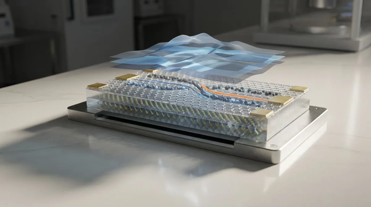
The central innovation in this research is to rethink the very nature of an electrical contact. Instead of using a traditional bulk metal, the researchers used another 2D material—graphene—as the electrode. They didn't just place it next to the MoS2; they created what is known as a vertical heterostructure by carefully stacking a layer of graphene directly on top of the MoS2 channel. This creates a pristine, atomically sharp interface between the two materials, free from the contamination and structural defects that often plague conventional metal contacts.
The real breakthrough occurs at this perfectly engineered interface. Due to the fundamental electronic properties of the two distinct materials, a phenomenon called interfacial charge transfer spontaneously occurs. In simple terms, electrons naturally flow from the graphene layer into the MoS2 layer right underneath it. This process effectively "dopes" the MoS2, enriching it with charge carriers precisely in the region where the electrical contact is made. This influx of carriers drastically lowers the energy barrier for current injection, essentially creating an electronic on-ramp where a tollbooth used to be. The result is a highly efficient, low-resistance contact that allows the transistor to operate closer to its full theoretical potential.
To understand the mechanics, we need to look at the structure of the field-effect transistor. A FET works like a switch, controlling the flow of current through a semiconductor channel by applying a voltage to a nearby gate. In this device, the channel is the MoS2 layer. The source and drain, which are the terminals for current entering and leaving the channel, are made from graphene. The genius of the vertical heterostructure design is that the graphene and MoS2 are in direct, van der Waals contact over a large surface area.
This intimate contact is what allows for the efficient charge transfer. Every material has a property called a "work function," which is the energy required to pull an electron out of its surface. The specific alignment of the work functions of graphene and MoS2 creates an energetic downhill slope for electrons, encouraging them to move from the graphene to the MoS2. This transfer of charge fundamentally changes the electronic landscape at the interface, effectively eliminating the Schottky barrier and forming what is known as an Ohmic contact. An Ohmic contact is the ideal for electronics—it behaves like a simple resistor, allowing current to flow smoothly without a significant energy penalty. This smooth flow is the basis for the "enhanced transport" described by the researchers. The quality of this interface is paramount, relying on the use of high-purity materials, such as those found in an industrial graphene supply, to ensure the desired electronic interactions can occur without disruption from impurities or defects.
The title of the paper highlights two key findings: enhanced charge transport and improved thermal stability. By fabricating and testing these graphene-MoS2 heterostructure transistors, the team was able to quantify these improvements. The "enhanced transport" manifested as superior device metrics compared to MoS2 transistors with traditional metal contacts. This would include significantly higher carrier mobility, meaning electrons could move through the MoS2 channel faster and with fewer obstacles. It also means a higher on-state current, allowing the transistor to deliver more processing power when active.
The second, and perhaps more crucial, finding was the device's exceptional thermal stability. Electronics are notoriously sensitive to temperature. In a typical silicon transistor, as temperature rises, its performance degrades; carrier mobility drops and leakage currents increase, wasting power and potentially leading to device failure. The researchers tested their heterostructure devices across a range of operating temperatures and found that they maintained their high performance far better than conventional devices. This robustness is attributed to the nature of the 2D-2D interface. The van der Waals bond between the graphene and MoS2 is physically stable and electronically consistent even as the device heats up. Furthermore, graphene's world-class ability to conduct heat may also play a secondary role in pulling thermal energy away from the active MoS2 channel, helping to keep it cool. This work is a significant contribution to the broader field of graphene electronics.
This research provides a powerful and elegant solution to the contact resistance problem that has long been a major obstacle for the entire field of 2D material electronics. By demonstrating the effectiveness of the graphene-MoS2 vertical heterostructure, it offers a scalable design principle for building high-performance, post-silicon devices. The implications are far-reaching. Overcoming the contact barrier unlocks the true potential of TMD semiconductors, paving the way for transistors that are smaller, faster, and more energy-efficient than what is possible with silicon today.
The enhanced thermal stability is particularly significant. In an era of massive data centers, high-performance computing, and power-hungry artificial intelligence hardware, managing heat is a multi-billion-dollar problem. Transistors that can operate reliably at elevated temperatures could reduce cooling costs, increase processing density, and enable new graphene applications in harsh environments, such as inside electric vehicle power systems, downhole drilling equipment, or aerospace control systems. This work moves the concept of 2D material electronics from a laboratory curiosity closer to a practical engineering solution.
While the scientific principles demonstrated in this study are sound, it is important to maintain perspective. This research represents a proof-of-concept, likely conducted on a small number of devices fabricated individually in a lab. The single largest barrier between this result and a commercial product is manufacturing scalability. The techniques used to exfoliate single atomic layers and precisely stack them on top of each other are difficult, time-consuming, and not yet suitable for mass production. Developing methods for growing large, uniform wafers of graphene and MoS2 and then transferring and patterning them with billion-transistor precision will require immense investment and innovation in graphene production machinery.
Furthermore, while the study demonstrated excellent short-term thermal stability, the long-term reliability of these devices over thousands of hours of operation under electrical and thermal stress is still an open question. Issues like interface degradation, material oxidation, and susceptibility to environmental factors will need to be thoroughly investigated. Finally, achieving consistent performance across millions of devices on a chip is a monumental challenge that the entire 2D materials community is working to solve.
Assuming the manufacturing challenges can be overcome, the technology demonstrated here could enable a new generation of electronic devices. The high carrier mobility and low resistance make these transistors ideal for high-frequency applications, potentially forming the backbone of future 6G and 7G communication systems. Their atomic thinness, flexibility, and transparency could lead to revolutionary products like foldable smartphones with seamless displays, wearable biosensors integrated into clothing, or transparent electronics embedded in windows or eyeglasses.
The exceptional thermal stability makes them a prime candidate for power electronics and systems destined for extreme environments. This could mean more efficient power converters for the electrical grid, more reliable control modules in cars and airplanes, and processors for space probes that can withstand intense temperature swings. Ultimately, the high efficiency of these devices could dramatically reduce the power consumption of everything from mobile phones to the massive data centers that power the cloud, contributing to a more sustainable technological future.
If you take away just one idea from this research, let it be this: by intelligently stacking different 2D materials, we can engineer unique properties at their interface that are impossible to achieve otherwise. Using graphene as an electrical contact for an MoS2 transistor creates a near-perfect junction, allowing for an automatic charge transfer that simultaneously boosts the device's speed and makes it remarkably resilient to heat, solving one of the biggest roadblocks for the future of electronics.
What is a heterostructure?
A heterostructure is a device made by stacking layers of different materials together. In this case, it is a "vertical heterostructure" because the layers of graphene and molybdenum disulfide are placed directly on top of one another. This stacking allows engineers to combine the best properties of each material and create new, emergent phenomena at the interface where they meet.
Why not just use graphene for the whole transistor?
While graphene is an extraordinary conductor of electricity, it naturally lacks a bandgap. A bandgap is the property that allows a material to be switched from a conducting 'on' state to a non-conducting 'off' state. Without a bandgap, you can't build a reliable digital switch. MoS2, as a semiconductor, has an excellent natural bandgap, making it perfect for the transistor's channel, while graphene's conductivity makes it perfect for the contacts.
What is "interfacial charge transfer"?
Interfacial charge transfer is the natural movement of electrons between two different materials when they are brought into intimate contact. This migration is driven by a difference in the materials' intrinsic electronic energy levels. In this research, electrons move from the graphene to the MoS2, which is a key part of what makes the electrical contact so efficient.
Is this technology ready for my smartphone?
No, not for a long time. This is foundational research that proves a scientific concept. The engineering challenges involved in manufacturing billions of these complex, perfectly aligned heterostructures reliably and affordably are immense. It will likely be many years, if not decades, before this type of technology finds its way into consumer electronics.
Why is thermal stability so important for electronics?
All electronic components generate waste heat during operation, and this heat degrades their performance and can lead to failure. A thermally stable transistor can maintain its speed and efficiency even as it gets hot. This is critical for high-performance computers, data centers that run 24/7, and electronics that must operate in hot environments like inside a car's engine compartment.
The work by Ashis Kumar Panigrahi and his colleagues provides a compelling demonstration of interface engineering at the atomic scale. By creating a vertical heterostructure of graphene and MoS2, they have not only fabricated a high-performance transistor but have also provided a clear blueprint for solving the persistent problem of contact resistance in 2D electronics. The resulting improvements in charge transport and thermal stability are not merely incremental; they represent a significant step toward realizing the promise of post-silicon computing. While the path to commercialization remains long and fraught with manufacturing hurdles, this research illuminates a scientifically elegant and powerful strategy for building the electronic devices of the future.
Serious about B2B integration? Test our premium Pulsed Electrical Resistive Carbon Heating turbostratic graphene in your lab. 100g sample packs available now.
Explore More
Researchers demonstrate a novel method for creating gate-tunable synthetic antiferromagnetism in a graphene-based heterostructure, paving the way for new...
Discover how a cellular automaton model for thermal transport offers a new, computationally efficient way to understand and engineer heat flow in graphene...
New research on the violation of Onsager reciprocity in graphene presents a thermomechanical proof for non-reciprocal energy flow, suggesting future...