
Unlocking Nanoscale Heat Flow: How Phonon Coherence Changes Everything
New research reveals that the wave-like coherence of phonons, not just their particle-like scattering, governs heat transport in nanostructures. This...
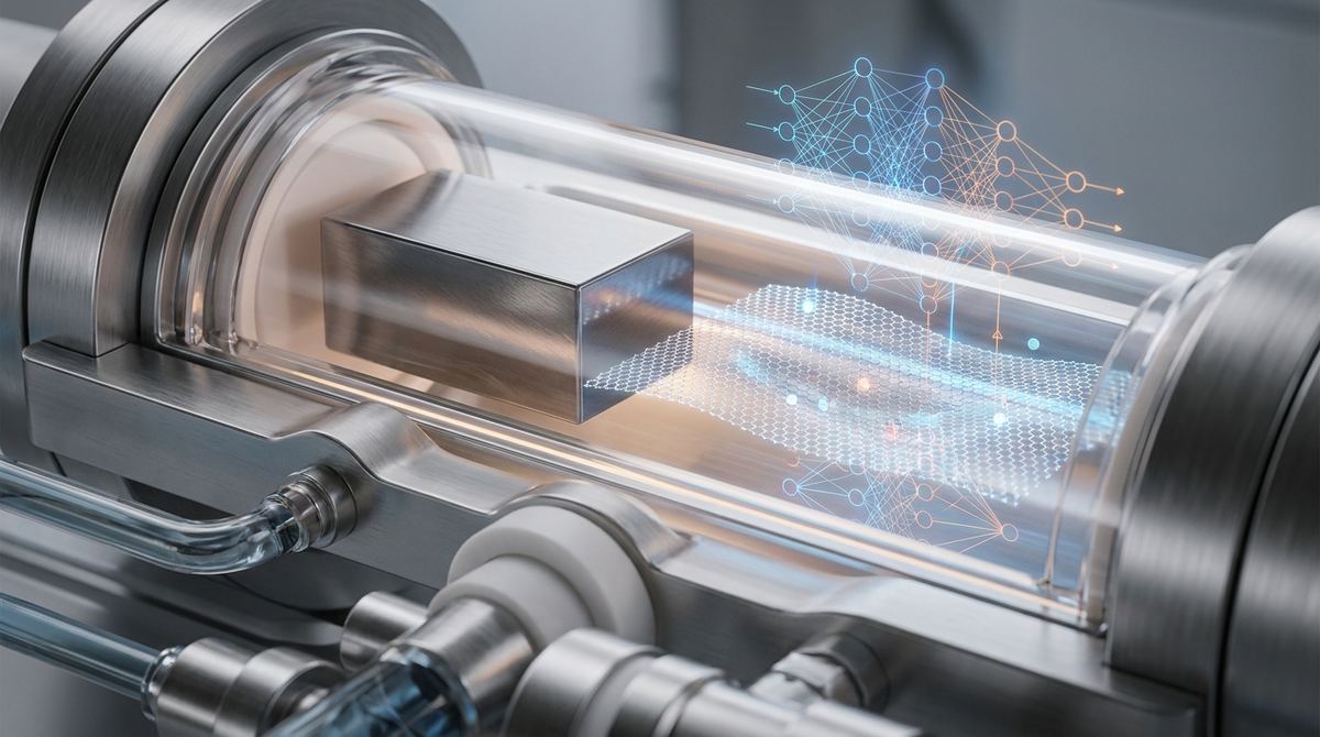
Imagine trying to tune a vast orchestra where you can only hear the average sound of all the instruments playing at once. You might know the overall performance is a little flat or sharp, but you have no way of knowing if the problem is a single violin or the entire brass section. For materials scientists working with graphene, this has been a persistent challenge. Graphene’s incredible electronic properties can be precisely tuned by intentionally introducing impurity atoms, a process called doping. However, understanding exactly how and where these dopants alter the material has been like listening to that chaotic orchestra. Now, a new approach combining advanced X-ray techniques with artificial intelligence is allowing scientists to finally isolate the sound of each instrument, providing a clear map of how individual dopants conduct their electronic symphony.
The ability to control graphene's electronic behavior is central to its promise for next-generation devices. Doping, the strategic replacement of carbon atoms with other elements like nitrogen or boron, is the primary method for this control. For example, nitrogen doping can introduce extra electrons, turning graphene into an n-type semiconductor, which is a fundamental building block for transistors and diodes. The problem is that doping is rarely a uniform process. Depending on the local chemical environment, a nitrogen atom can bond to the graphene lattice in several different ways, such as in a "graphitic," "pyridinic," or "pyrrolic" configuration. Each of these bonding types has a unique and distinct effect on the local electronic structure. Traditional characterization methods often measure the bulk properties of the material, averaging the effects of all these different dopant sites together. This gives an incomplete, and often misleading, picture. Without a way to see the precise location and electronic impact of each type of dopant, engineers cannot rationally design and reliably manufacture high-performance graphene devices. It creates a bottleneck, slowing the transition from laboratory potential to industrial reality.
The research by Yinan Wang, Arpita Varadwaj, Teruyasu Mizoguchi, and Masato Kotsugi introduces a powerful method to overcome this characterization hurdle. Their core idea is to combine a highly sensitive atomic probe with the pattern-recognition power of machine learning. They use a technique called X-ray Absorption Near Edge Structure, or XANES, which acts like a highly specific fingerprinting tool. By tuning an X-ray beam to the right energy, they can make it interact almost exclusively with the dopant atoms, like nitrogen. The way the X-rays are absorbed reveals detailed information about that specific atom's chemical bonding and electronic state. Crucially, they don't just take one measurement for the whole sample. They use a microscopic X-ray beam to scan across the graphene surface, collecting a full XANES fingerprint at every single pixel. This generates a massive, complex dataset. The final piece of the puzzle is machine learning. The researchers train a computational model to sift through these thousands of spectral fingerprints, learn the subtle differences between them, and automatically classify each region of the graphene sheet. The result is a detailed map that decodes the complex landscape of the material, showing precisely where each type of dopant is located and what it is doing to the material’s electronic properties.
The experimental process is a sophisticated fusion of physics and data science. It begins with the synthesis of a doped graphene sample, for instance, a single layer of graphene grown via chemical vapor deposition where nitrogen gas is introduced during the process. This material, which may contain a mix of different nitrogen bonding configurations, is the subject of the investigation. The sample is then taken to a synchrotron, a massive facility that produces exceptionally bright and finely-tuned X-ray beams, far more powerful than those used in a hospital. The technique employed is a variant of XANES, likely Scanning Transmission X-ray Microscopy (STXM), which combines spectroscopy with imaging. An X-ray beam is focused down to a spot just nanometers wide and scanned across the graphene sheet in a grid pattern. At each point in the grid, the energy of the X-ray beam is swept through a range corresponding to the nitrogen atom's core electron absorption edge. This process generates an absorption spectrum, a graph showing how much the X-rays were absorbed at each energy. This spectrum is the unique fingerprint that reveals the local chemical environment of the nitrogen atoms at that specific spot. Repeating this for thousands of points creates a hyperspectral data cube—a stack of images where each pixel contains not just an intensity value, but a full XANES spectrum. This dataset is far too complex for simple visual inspection, which is where machine learning comes in. The researchers can use unsupervised learning algorithms, which are designed to find hidden patterns in data without prior labeling. The algorithm groups pixels with similar spectral features together into distinct clusters. Each cluster corresponds to a specific type of nitrogen dopant configuration and its associated electronic structure.
The title of the paper, "Decoding Dopant-Induced Electronic Modulation," strongly suggests the success of this combined approach. By applying their machine learning model to the XANES data, the researchers were able to produce a spatially resolved map of the doped graphene. This map is not just a picture; it is a quantitative chart that distinguishes regions dominated by graphitic nitrogen from those with pyridinic nitrogen or other bonding types. The model effectively learned to connect subtle shifts and changes in the shape of the XANES spectra to these specific chemical states. More importantly, they were able to correlate these identified regions with specific "electronic modulations." This means they could determine how each type of dopant site altered key electronic properties, such as the local density of states or the position of the Fermi level. For example, they could quantitatively demonstrate that one type of nitrogen site is more effective at donating electrons to the graphene lattice than another. In essence, they moved beyond a simple average and created a detailed, localized understanding of the structure-property relationship in a real-world, imperfectly doped material. This provides a direct visual and quantitative link between the atomic-scale chemistry and the functional electronic properties of the graphene sheet.
This work represents a significant leap forward in the characterization of 2D materials. For engineers and scientists developing graphene electronics, this method provides an unprecedented diagnostic tool. Instead of relying on trial and error, they can now visualize how different synthesis conditions affect the distribution and type of dopants. This accelerates the development of reliable manufacturing protocols for creating graphene with tailored electronic properties. For example, in creating a graphene-based transistor, it is crucial to have uniform doping to ensure predictable performance across a silicon wafer. This technique allows researchers to inspect their materials and identify sources of non-uniformity, leading to higher quality and better device yields. It transforms materials characterization from a "black box" problem into a transparent, data-driven science. This ability to see and understand heterogeneity at the nanoscale is fundamental to quality control and rational material design, closing the gap between the theoretical promise of doped graphene and its practical, high-performance applications. It allows for a more precise and deterministic approach to engineering the building blocks of future electronic and quantum devices.
While incredibly powerful, this methodology has its limitations. The primary constraint is its reliance on synchrotron light sources. These are large, expensive, and highly specialized facilities with limited access, meaning the technique is not suitable for routine, high-throughput quality control on a factory floor. It is currently a tool for fundamental research and advanced development rather than mass production. Furthermore, the machine learning model's accuracy is entirely dependent on the quality and interpretation of the XANES data. Any artifacts or noise in the spectral measurements could be misinterpreted by the algorithm, leading to incorrect classifications. The study likely focused on a specific dopant, such as nitrogen. The effectiveness of the technique and the specific machine learning models would need to be validated for other important dopants like boron, phosphorus, or sulfur, each of which presents its own unique spectral signatures and challenges. Finally, this work provides a static snapshot of the material. Future work could explore in-situ or in-operando measurements, observing how the dopant configurations and their electronic effects change in real-time under operating conditions, such as when a voltage is applied or when exposed to a chemical analyte.
The direct implications of this research span several high-value sectors. In the semiconductor industry, this method can accelerate the development of graphene-based field-effect transistors (FETs) by enabling the precise engineering of p-n junctions, which are the basis of all modern electronics. By mapping the dopant landscape, manufacturers can ensure the uniformity and reliability required for complex integrated circuits. For the sensor industry, the performance of graphene sensors often depends on the presence of specific defect or dopant sites that act as active locations for binding target molecules. This technique allows for the direct imaging of these active sites, enabling a more rational design of sensors with higher sensitivity and selectivity for detecting specific gases or biomolecules. In the field of catalysis, doped graphene is a promising metal-free catalyst. The catalytic activity is highly dependent on the local electronic structure at the dopant sites. This research provides a direct method to identify and quantify the most active sites, guiding the synthesis of more efficient catalysts for energy conversion and chemical production. Finally, for producers of bulk graphene materials like turbostratic graphene flakes, advanced characterization methods derived from this work could eventually lead to more robust quality control metrics, providing customers with materials that have more consistent and well-defined properties.
If you take away just one idea, let it be this: by combining advanced X-ray vision with the pattern-finding power of artificial intelligence, scientists can now create detailed maps that show exactly how and where individual impurity atoms tune the electronic properties of graphene, paving the way for more deliberate and precise engineering of next-generation materials.
What is doping in the context of graphene? Doping is the intentional introduction of impurities into a material to change its properties. In graphene, which is made of carbon atoms, doping involves replacing some carbon atoms with atoms of another element, like nitrogen or boron. This changes the number of available charge carriers (electrons or holes) in the graphene, allowing scientists to fine-tune its conductivity and turn it into a semiconductor, which is essential for building electronic components.
What is XANES and why is it useful here? XANES stands for X-ray Absorption Near Edge Structure. It is a highly sensitive spectroscopy technique that uses finely-tuned X-rays to probe the electronic structure and chemical environment of a specific element. It acts like an atomic fingerprint. By tuning the X-rays to the energy specific to the dopant atom, scientists can learn exactly how it is bonded within the graphene lattice and what effect it is having on the electrons around it.
Why is machine learning necessary for this analysis? When XANES is used to scan a surface, it produces a massive and complex dataset containing thousands of individual spectra, one for each point on the map. It is practically impossible for a human to manually analyze all this data and spot the subtle patterns. A machine learning algorithm can process this entire dataset, identify hidden similarities between the spectra, and automatically group them, effectively decoding the complex information into a clear and understandable map of the material's properties.
Is this technology ready for industrial quality control? Not directly in its current form. The technique relies on large, expensive research facilities called synchrotrons, which are not practical for a factory setting. However, the insights gained from this advanced method can be used to develop and calibrate more accessible, lab-scale or industrial-scale characterization tools. It serves as a "gold standard" reference that can help create faster and cheaper quality control methods down the line.
What does "electronic modulation" mean in simple terms? Electronic modulation simply means changing or controlling the electronic properties of a material. For graphene, this could mean making it more or less conductive, opening up an energy gap to make it behave like a semiconductor, or creating specific sites that are more chemically reactive. The dopant atoms are the "modulators" that allow scientists to dial in these properties for a specific application.
The work by Wang, Varadwaj, Mizoguchi, and Kotsugi provides a critical new lens through which to view and understand the atomic-scale intricacies of doped graphene. By successfully pairing region-resolved XANES with machine learning, they have created a methodology that moves beyond simple bulk characterization to reveal the rich, heterogeneous landscape of dopant-induced electronic effects. This is not merely an academic achievement; it is a foundational enabling technology. It provides the clear, actionable feedback needed to refine synthesis processes, control material quality, and design graphene-based devices with a level of precision that was previously out of reach. As the demand for more powerful and efficient electronics, sensors, and catalysts grows, this ability to decode and engineer materials at their most fundamental level will be indispensable in turning the remarkable promise of graphene into a tangible reality.
Serious about B2B integration? Test our premium Pulsed Electrical Resistive Carbon Heating turbostratic graphene in your lab. 100g sample packs available now.
Explore More
New research reveals that the wave-like coherence of phonons, not just their particle-like scattering, governs heat transport in nanostructures. This...

Researchers show deep-UV bleaching of charge disorder in encapsulated graphene, a novel technique that uses light to erase electrical noise and improve...

Scientists have found evidence of a metallic Wigner crystal in rhombohedral graphene, a paradoxical state where electrons freeze into a solid but can still...