
Metallic Wigner Crystal Discovered in Rhombohedral Graphene
Scientists have found evidence of a metallic Wigner crystal in rhombohedral graphene, a paradoxical state where electrons freeze into a solid but can still...
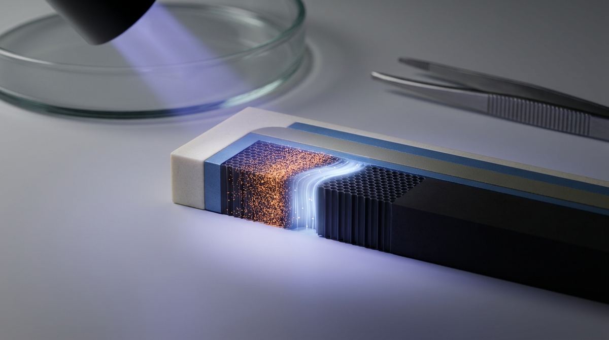
Imagine trying to listen to a faint, distant signal on an old radio filled with static. The noise floor is so high that the actual information is lost in the hiss and crackle. For scientists and engineers developing next-generation electronics, graphene often presents a similar challenge. While its theoretical potential is immense—offering unparalleled electron speed and efficiency—real-world devices are plagued by a form of electrical "static" known as charge disorder. This background noise, arising from microscopic imperfections, scatters electrons and throttles performance. A new technique, however, offers a way to turn down the static. Groundbreaking research demonstrates that a simple flash of deep-ultraviolet light can effectively "bleach" away this disorder, cleaning the electrical environment and unlocking a much higher level of performance in graphene devices.
To achieve its highest potential, graphene must be kept pristine. Any contact with the outside world introduces contaminants that degrade its remarkable electronic properties. The gold standard for protecting it is encapsulation, where a single sheet of graphene is sandwiched between two atomically flat layers of an insulating material called hexagonal boron nitride (hBN). This creates a van der Waals heterostructure, a clean and protected environment where electrons can move with incredible speed. However, the fabrication process itself, which involves manually stacking these atomic layers, inevitably traps impurities at the interfaces. These impurities can be leftover polymer residues from the transfer process or other airborne molecules. Each impurity carries a small electrical charge, creating a random, bumpy electrical landscape across the graphene sheet. This landscape of "charge puddles" acts like a field of potholes for the electrons trying to flow through the material. Instead of moving in a straight line, they scatter, slowing down and losing energy. This phenomenon, known as charge disorder, is a fundamental roadblock. It limits electron mobility, which directly impacts the maximum operating speed of a transistor, and it creates significant device-to-device variability, a fatal flaw for commercial manufacturing. Research from a team including Daniil Domaretskiy, Ned Hayward, Van Huy Nguyen, Simone Benaglia, Kornelia Indykiewicz, Hadrien Vignaud, Jing Zhang, Kenji Watanabe, Takashi Taniguchi, V. I. Fal'ko, Laura Fumagalli, and L. A. Ponomarenko, et al., directly confronts this long-standing challenge with an elegant and non-invasive solution.
The central idea behind this work is to use light as a cleaning tool. Specifically, the researchers used deep-ultraviolet (DUV) light, which consists of photons with very high energy. The hypothesis was that these energetic photons could penetrate the top hBN layer and interact with the trapped impurities at the graphene-hBN interface without damaging the device's structure. This interaction could work in two ways. First, the DUV energy could be sufficient to neutralize the trapped electrical charges, effectively "smoothing out" the electrical potholes. Second, it could break down the chemical bonds of residual organic contaminants, like polymers, rendering them inert. The process is aptly named "bleaching" because it's analogous to how light can break down colored dye molecules to remove a stain. Here, the "stain" is the electrical noise, and the DUV light is the cleaning agent. By applying this light treatment after the device is fully fabricated, it serves as a simple and effective post-processing step to significantly improve the quality and performance of the encapsulated graphene.
The devices at the heart of this study are state-of-the-art graphene heterostructures. The fabrication begins by exfoliating, or peeling off, single-atom-thick layers of graphene and hBN from bulk crystals. Using a meticulous process under a microscope, a flake of graphene is picked up and placed on top of a flake of hBN. Then, another hBN flake is placed on top of the graphene, creating the protective sandwich structure. This entire stack is then placed on a silicon wafer that serves as a substrate and a back gate, which allows an electric field to be applied to control the number of charge carriers (electrons or holes) in the graphene. Metal contacts are then patterned onto the device to allow for electrical measurements. The result is a graphene field-effect transistor, the fundamental building block of modern electronics.
The key to the experiment is the measurement of the device's electronic properties before and after the DUV treatment. The researchers first characterize the initial state of the device by measuring its resistance as they vary the gate voltage. This produces a characteristic curve with a peak at the "Dirac point," which is the point of minimum conductivity. The width and height of this peak are direct indicators of the amount of charge disorder; a wide, low peak signifies a messy, disordered system, while a sharp, high peak indicates a clean, uniform one. After this initial measurement, the device is placed in a vacuum chamber and illuminated with a DUV lamp for a specific duration. Following the illumination, the electrical measurements are repeated to quantify the change in device quality.
The results were a clear and compelling validation of the DUV bleaching concept. After exposure to the deep-UV light, the electronic characteristics of the encapsulated graphene devices improved dramatically. The resistance peak at the Dirac point became significantly sharper and narrower, a textbook signature of reduced charge disorder. This indicates that the DUV light successfully smoothed out the random potential fluctuations, creating a much more uniform electrical environment for the charge carriers.
This homogenization of the electrical landscape had a direct and profound effect on performance. The researchers observed a substantial increase in carrier mobility, the metric that quantifies how easily electrons can move through the material. In essence, by "repaving" the electronic roadway, the electrons could travel much faster with fewer scattering events. The effect was also found to be stable and persistent long after the DUV light was switched off, suggesting a permanent or semi-permanent modification of the trapped impurities. The study likely explored the optimal dosage of DUV light, finding a sweet spot where the cleaning effect is maximized without introducing new photo-induced defects into the crystal lattice, which could happen with excessive exposure. This demonstrates a controllable, post-fabrication method to reliably elevate the quality of graphene electronic devices.
This work is significant because it offers a practical solution to one of the most persistent problems in the field of graphene electronics. Fabricating perfectly clean heterostructures is incredibly difficult, time-consuming, and suffers from low yield. Many promising laboratory results are hard to reproduce simply because of uncontrolled variations in contamination. The DUV bleaching technique provides a much-needed "reset button." It allows researchers to take an already fabricated, and perhaps mediocre, device and elevate its performance to a much higher standard.
This has profound implications for both fundamental science and commercial technology. For scientists, it provides a tool to systematically remove extrinsic disorder, allowing them to study the intrinsic, fundamental physics of graphene and other 2D materials more clearly. For engineers, it addresses the critical issue of device uniformity. If you can reliably clean up devices after they are made, you can achieve much tighter performance specifications across a whole wafer of chips. This is a crucial step toward scalable manufacturing. By providing a simpler, more accessible alternative to complex methods like high-temperature thermal annealing, this technique could accelerate the entire development cycle for advanced graphene-based technologies.
While incredibly promising, this research represents an early-stage proof of concept, and several questions remain. The experiments were conducted on individual, small-scale devices in a laboratory setting. A critical next step is to demonstrate that this technique is scalable and can be applied uniformly across a large-area wafer, which is a prerequisite for any industrial process. The long-term stability of the bleached state also needs more rigorous investigation. While the initial results show persistence, it is crucial to understand if the charge disorder can slowly return over months or years, or under the stress of real-world operating conditions such as high temperatures and strong electric fields.
Furthermore, while the hypothesis of neutralizing trapped charges and breaking down polymers is strong, the precise chemical and physical mechanisms at play require deeper study. Advanced characterization techniques could help pinpoint exactly what is happening at the atomic scale at the graphene-hBN interface during DUV exposure. Finally, researchers will need to explore the applicability of this method to a wider range of 2D material heterostructures and more complex device geometries. Understanding the boundaries and optimal parameters of this technique will be essential for its widespread adoption.
If this technique can be matured and scaled, its impact on technology could be widespread. The primary beneficiary would be high-frequency electronics for next-generation communication systems, like 6G and beyond. The increased electron mobility directly translates to faster transistors, enabling circuits that can operate at terahertz frequencies. Another major area is in the realm of highly sensitive graphene sensors. By reducing the intrinsic electrical noise, the signal-to-noise ratio of sensors designed to detect minute quantities of chemicals or biological molecules could be dramatically improved.
In quantum computing, where the fragile quantum states of qubits are easily disturbed by environmental noise, creating an ultra-clean electronic environment is paramount. DUV bleaching could become a standard procedure for preparing graphene-based quantum devices, improving their coherence times and reliability. Ultimately, this work contributes to the broader ecosystem of advanced materials and the diverse applications they enable, from ultra-fast computing to novel medical diagnostics.
If you take away just one idea from this research, it should be this: A simple, post-fabrication treatment with deep-ultraviolet light can act as a powerful cleaning process for high-performance graphene devices, erasing inherent electrical noise and significantly boosting their speed and reliability.
What is charge disorder in graphene?
Charge disorder refers to random, microscopic variations in the electrical potential across a sheet of graphene, often described as "charge puddles." It's caused by charged impurities trapped near the graphene, typically during the device fabrication process. This uneven electrical landscape acts as an obstacle course for electrons, scattering them and limiting the device's overall performance.
Why is encapsulated graphene used in this research?
Encapsulated graphene, where a graphene sheet is sandwiched between two layers of an insulator like hexagonal boron nitride (hBN), represents the highest-quality platform for graphene electronics. The hBN provides an atomically smooth surface and protects the graphene from environmental contaminants, allowing electrons to move with very little disruption and unlocking its superior electronic properties.
What is "deep-UV bleaching" in this context?
Deep-UV (DUV) bleaching is the process of using high-energy ultraviolet light to clean up the charge disorder within an encapsulated graphene device. The energetic DUV photons are thought to neutralize trapped electrical charges and break down residual organic molecules at the interface between the graphene and the hBN, effectively smoothing out the electrical landscape without damaging the device.
Is this technology ready for commercial use in electronics?
No, this technology is currently at the laboratory proof-of-concept stage. While the results are very promising, significant research and development are needed to test its long-term stability, understand the underlying mechanisms more deeply, and, most importantly, prove that the process can be scaled up for reliable, large-area manufacturing on industry-standard wafers.
How does reducing charge disorder improve graphene electronics?
Reducing charge disorder directly improves two key metrics. First, it increases carrier mobility, meaning electrons can travel faster and with fewer interruptions, which is essential for creating faster transistors for high-frequency applications. Second, it improves device uniformity, meaning different devices fabricated on the same chip will behave more predictably, which is a critical requirement for any viable commercial manufacturing process.
The work by Daniil Domaretskiy and his collaborators provides an elegant and powerful new tool in the quest to harness the full potential of graphene. By demonstrating that deep-UV light can effectively erase the charge disorder that has long plagued even the highest-quality devices, they have opened a new pathway toward more reliable and higher-performing graphene electronics. This non-invasive, post-fabrication cleaning technique addresses a critical bottleneck, potentially accelerating the transition of graphene from a material of scientific wonder to a cornerstone of future technology. While the path to industrial-scale implementation requires further work, this research marks a significant and encouraging step forward, shining a light—quite literally—on a solution to one of graphene’s most persistent challenges.
Serious about B2B integration? Test our premium Pulsed Electrical Resistive Carbon Heating turbostratic graphene in your lab. 100g sample packs available now.
Explore More
Scientists have found evidence of a metallic Wigner crystal in rhombohedral graphene, a paradoxical state where electrons freeze into a solid but can still...

Researchers predict a new state of matter in rhombohedral graphene: the metallic Wigner crystal. This paradoxical phase, where electrons are both frozen and...

Researchers show how dielectric substrates can control ultrafast carrier dynamics in graphene, offering a new method for designing next-gen terahertz and...