
Modeling Electron Transport in 2D Materials with New Boltzmann Equations
Researchers developed coupled dynamical Boltzmann transport equations that include long-range interactions, creating a more accurate model for electron...
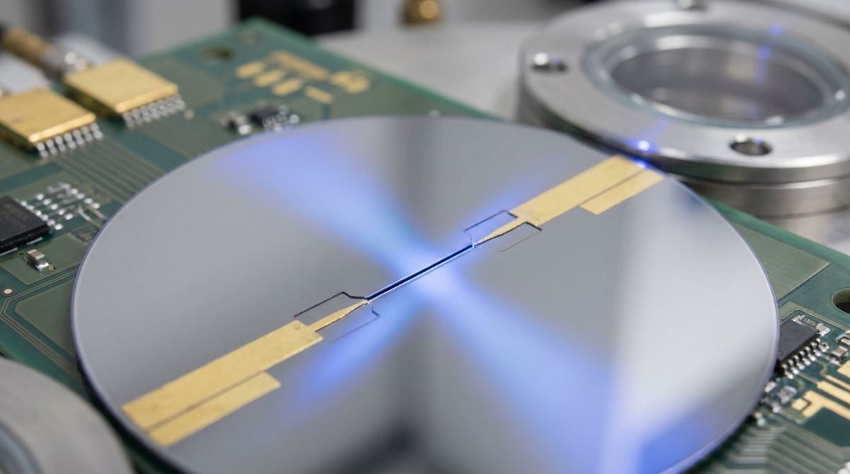
The field of nanoelectronics is currently undergoing a paradigm shift from classical charge-based transport to quantum-wave-based transport. As transistors shrink to the atomic scale, the wave-like nature of electrons becomes impossible to ignore. This transition opens the door to electron quantum optics, where electrons are manipulated much like photons in a fiber-optic system.
Recent research, specifically the work by Rhanbouri, Pasek, and El Fatimy, has identified a highly efficient geometry for this manipulation: the graphene slit junction. This device structure allows for the formation of directional electron beams, coherent interference patterns, and, most importantly, the ability to filter electrons based on their spin. For engineers and startups working in the quantum computing or advanced sensing sectors, mastering the fabrication of these slit junctions is a critical step toward developing next-generation spintronic and quantum logic components.
This guide provides a practical roadmap for prototyping a graphene slit junction device, moving from theoretical concepts to a physical laboratory setup.
To build a functional device, one must understand the physics that makes the slit junction unique. In standard conductors, electrons move in a diffusive manner, scattering off impurities and boundaries. However, in a carefully engineered graphene slit junction, we can exploit specific quantum mechanical effects to control electron flow.
The first key effect is trigonal warping. In monolayer graphene, the energy dispersion relation is not perfectly circular; it possesses a three-fold symmetry known as trigonal warping. At specific energy levels, particularly around 2.7 eV, this warping causes the electron wavefunctions to become highly directional. Instead of spreading out in all directions, the electrons are channeled into specific beams.
The second effect is the Aharonov-Bohm effect. When electrons travel through a slit or around a magnetic flux, the magnetic field shifts the phase of the electron wavefunction. This results in measurable oscillations in the electrical conductance of the device. By modulating the magnetic flux, we can control the interference of the electron waves, effectively creating a transistor that is controlled by magnetic fields rather than just electric ones.
The third effect is spin filtering. In its natural state, graphene is antiferromagnetic, meaning the spin-up and spin-down electrons are degenerate and move through the device identically. However, by breaking the left-right symmetry of the slit—either through structural changes or by applying a local electrostatic gate—we can force the device to transmit one spin state while blocking the other. This is the fundamental requirement for a spin-based logic gate.
Because the research involves complex atomistic tight-binding calculations, translating these results into a physical prototype requires several engineering assumptions.
First, we must address the energy levels. The research notes that monolayer graphene produces strong directional beams at 2.7 eV. This is a very high energy level for standard nanoelectronics and may require specialized high-energy injection techniques. However, the research also demonstrates that bilayer graphene can achieve analogous beam formation at much lower energies, specifically around 50 meV.
For a practical laboratory prototype, we recommend focusing on the bilayer graphene implementation. Operating at 50 meV is significantly more manageable with standard cryogenic measurement equipment and reduces the risk of dielectric breakdown in the gate oxides.
Second, the slit dimensions are critical. While the research uses theoretical models, a physical prototype will require a slit width in the range of 50 nm to 200 nm. Anything wider will lose the quantum interference effects, and anything narrower may become too difficult to fabricate reliably using standard electron-beam lithography.
Third, the symmetry-breaking mechanism. To achieve spin filtering, the device must have an asymmetric potential. We assume the use of a local electrostatic gate positioned near one side of the slit to provide this asymmetry.
Building a device at this scale requires a high-end nanofabrication facility. The following materials and tools are essential for a successful prototype.
Materials:
1. High-quality monolayer or bilayer graphene: CVD-grown graphene on a silicon/silicon dioxide (Si/SiO2) substrate is the industry standard.
2. Resist: PMMA (Polymethyl methacrylate) for electron-beam lithography.
3. Etchant: Oxygen plasma for the dry etching of the graphene.
4. Metallization: Titanium (Ti) and Gold (Au) for high-conductivity electrical contacts.
5. Substrate: Highly doped Silicon (acting as a back-gate) with a thin SiO2 layer (typically 285 nm or 90 nm).
Equipment:
1. Electron-Beam Lithography (EBL) system: Necessary for defining the nanometer-scale slit.
2. Reactive Ion Etcher (RIE): For precise oxygen plasma etching of the graphene.
3. Electron-Beam Evaporator: For depositing the metal contacts.
4. Cryogenic Probe Station: To perform measurements at low temperatures (essential for observing quantum interference).
5. High-precision Magnet: To apply the magnetic flux required for Aharonov-Bohm oscillations.
For those looking to scale this process, investing in advanced /equipment/ such as pulsed electrical reactors or high-precision EBL systems is vital for moving from a single prototype to industrial-scale production.
The following steps outline the standard nanofabrication workflow for creating a graphene slit junction.
1. Substrate Preparation and Graphene Transfer
Begin with a clean Si/SiO2 substrate. The graphene should be transferred onto the substrate using the PMMA-assisted transfer method. Once transferred, the substrate must be cleaned using a mild oxygen plasma to remove any residual PMMA or organic contaminants.
2. Electron-Beam Lithography (EBL) for Slit Patterning
This is the most critical step. Spin-coat a thin layer of PMMA over the graphene. Use an EBL system to expose a narrow line that represents the slit. The dose must be carefully calibrated to ensure the slit width is consistent and the edges are sharp. Sharp edges are vital; any roughness at the slit boundary will cause uncontrolled scattering and destroy the quantum interference patterns.
3. Oxygen Plasma Etching
After developing the PMMA resist, subject the sample to oxygen plasma etching. This will remove the graphene in the exposed areas, creating the slit. The etching time must be precisely controlled to ensure the slit reaches the full depth of the graphene layer without damaging the underlying SiO2.
4. Contact Deposition
To measure the device, you need electrical contacts at both ends of the slit. Use an electron-beam evaporator to deposit a layer of Titanium (for adhesion) followed by a thicker layer of Gold. These contacts should overlap the graphene edges to ensure low-resistance ohmic contact.
5. Integration of the Local Gate
To enable the spin-filtering and phase-control capabilities described in the research, a local electrostatic gate is required. This can be achieved by using a secondary, smaller slit or a patterned gate electrode placed directly beneath or near the junction. This gate allows you to tune the interference phase and break the symmetry of the device.
Once the prototype is fabricated, it must be tested to confirm that it behaves as a quantum optical element.
1. Conductance vs. Gate Voltage
First, perform a standard four-probe conductance measurement. By sweeping the back-gate voltage, you can map the carrier density. This helps confirm the quality of the graphene and the effectiveness of the slit in modulating current.
2. Aharonov-Bohm Oscillation Test
Apply a perpendicular magnetic field using your cryogenic probe station. As the magnetic field increases, you should observe periodic oscillations in the conductance. The period of these oscillations should correspond to the magnetic flux quantum (h/e). If these oscillations are present, it confirms that the electrons are traveling through the slit in a coherent, wave-like manner.
3. Spin-Filtering Verification
This is the most advanced test. To verify spin filtering, you must break the symmetry of the device using the local gate. By applying a specific voltage to the local gate, you should observe a change in the conductance that is not purely charge-dependent. In a highly optimized device, the conductance should become sensitive to the spin orientation of the electrons, effectively acting as a spin-valve.
4. Fourier Analysis of Oscillations
To confirm the results match the theoretical models, perform a Fourier analysis on the conductance-magnetic field data. The presence of specific harmonics in the Fourier spectrum will indicate the presence of higher-order interference effects and confirm the validity of the slit geometry.
Fabricating quantum-scale devices is fraught with technical risks.
Edge Roughness: As mentioned, the edges of the slit are the primary source of electron scattering. If your device shows no interference, the first thing to check is the quality of your plasma etch. Using a lower power, longer duration etch can sometimes produce smoother edges than a high-power, short-duration etch.
Thermal Decoherence: Quantum interference is extremely sensitive to temperature. If the temperature is too high, thermal fluctuations will wash out the Aharonov-Bohm oscillations. Always perform your primary testing at liquid helium temperatures (4.2K) or lower.
Material Impurities: Any impurities trapped in the graphene or at the substrate interface will act as scattering centers. Using high-purity CVD graphene and ensuring a pristine substrate environment is essential.
Scaling and Market Viability: While a single lab prototype is a scientific achievement, moving toward commercial applications requires a shift in focus. As the technology matures, the focus will shift from EBL-based fabrication to more scalable methods like /blog/category/graphene-production/ techniques. Understanding the /market-research/ regarding graphene pricing trends and commercial forecasts will be essential for any startup looking to move from the lab to the factory.
The graphene slit junction represents a powerful tool for the next generation of nanoelectronics. By combining the unique properties of graphene—such as trigonal warping and high carrier mobility—with precise geometric engineering, we can create devices that control electrons with the same precision we currently apply to light.
Whether you are building a prototype for a quantum logic gate or a highly sensitive magnetic sensor, the principles of electron quantum optics provide a robust framework. By following the fabrication and testing protocols outlined in this guide, researchers and engineers can begin to explore the vast potential of these tunable, spin-dependent quantum devices.
For related commercial context, explore graphene production machinery and graphene market research.
Serious about B2B integration? Test our premium Pulsed Electrical Resistive Carbon Heating turbostratic graphene in your lab. 100g sample packs available now.
Explore More
Researchers developed coupled dynamical Boltzmann transport equations that include long-range interactions, creating a more accurate model for electron...

Researchers have developed a hydrodynamic backflow method to ease the fermion sign problem, a major hurdle in quantum simulations of materials like graphene.

Learn to build a prototype active graphene metasurface for mid-IR beam steering. This guide covers the materials, fabrication, and testing for LiDAR.