
Hydrodynamic Backflow for Easing the Fermion Sign in Finite-Temperature Electron
Researchers have developed a hydrodynamic backflow method to ease the fermion sign problem, a major hurdle in quantum simulations of materials like graphene.
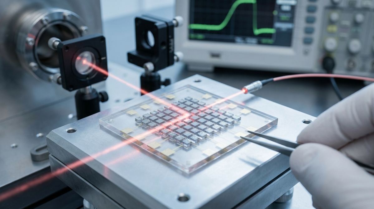
Spatial Light Modulators, or SLMs, are the engines behind technologies that precisely control light, from holographic displays to advanced imaging systems. In the world of Light Detection and Ranging (LiDAR), the ability to steer a laser beam without any moving parts is a revolutionary goal. Traditional SLMs are often bulky and slow. A new class of devices, called active metasurfaces, promises to change this by manipulating light at a subwavelength scale.
This guide provides a practical framework for prototyping a transmissive, graphene-based active metasurface designed for the mid-infrared (mid-IR) spectrum. Our project is based on the theoretical work presented by Christopher M. Yi and his colleagues in their 2026 paper, "Independent Amplitude and Phase Modulation in Active Transmissive Metasurfaces via Complex Permittivity Tuning." We will translate their theoretical model into a tangible set of steps for a small lab or startup looking to experiment with this cutting-edge technology. It is crucial to note that this guide is an interpretation of a theoretical study; the goal is to build and test a physical device that explores the principles outlined by the researchers.
The device we aim to build is a flat, transparent component that can dynamically alter the phase of a mid-IR laser beam passing through it. By controlling the phase of light across an array of tiny, individual "pixels," or unit cells, we can construct a wavefront that steers the beam in a desired direction. This is the core principle of a phased array, but implemented on an optical chip.
The key innovation here is the combination of two materials with unique electro-optical properties:
1. Germanium (Ge): A high-refractive-index semiconductor that is transparent in the mid-IR. We will structure it into an array of microscopic cuboid resonators. The specific geometry of these resonators creates a sharp optical resonance, making them highly sensitive to small changes in their environment.
2. Graphene: A single layer of carbon atoms with extraordinary electronic properties. By applying a small voltage to a graphene stripe integrated with each germanium resonator, we can dramatically change how the graphene interacts with light. This change is what tunes the metasurface.
Our goal is to fabricate a small array of these Ge-graphene unit cells and demonstrate that we can independently control the phase of transmitted light, enabling a basic beam-steering function.
This is an advanced nanofabrication project that requires a cleanroom environment and specialized equipment. This is not a hobbyist-level build.
Materials:
Substrate: 4-inch prime-grade Calcium Fluoride (CaF2) wafer. CaF2 is an excellent choice for its transparency deep into the mid-IR spectrum. Fused silica can be a less expensive alternative for near-IR work but is not suitable for the target mid-IR application.
Active Layer: High-quality, single-layer graphene grown via Chemical Vapor Deposition (CVD) on copper foil. The quality and uniformity of the graphene are paramount to device performance.
Resonator Material: High-purity (99.999%) germanium sputtering target or evaporation pellets.
Dielectric Layer: Precursors for Atomic Layer Deposition (ALD), such as Trimethylaluminum (TMA) for Aluminum Oxide (Al2O3) or Tetrakis(dimethylamido)hafnium(IV) for Hafnium Oxide (HfO2). Al2O3 is a common and reliable choice.
Electrodes and Heaters: High-purity gold (Au) and a suitable adhesion layer like chromium (Cr) or titanium (Ti).
Chemicals: Standard cleanroom solvents (acetone, isopropyl alcohol, deionized water), photoresists, e-beam resists (e.g., PMMA), and developers.
Equipment:
Lithography: An electron-beam (e-beam) lithography system is essential for defining the nanoscale features of the resonators and graphene stripes. A high-resolution photolithography stepper could be used for larger features like contact pads.
Deposition: An ALD system for the gate dielectric, an e-beam or thermal evaporator for metals, and a sputter deposition system for the germanium.
Etching: A Reactive Ion Etching (RIE) or Inductively Coupled Plasma (ICP-RIE) system with fluorine-based (e.g., SF6, CHF3) and oxygen (O2) chemistries.
Graphene Handling: A dedicated setup for wet or dry transfer of CVD graphene.
Metrology: Atomic Force Microscope (AFM) and Scanning Electron Microscope (SEM) for process control and inspection. Ellipsometer for measuring film thicknesses.
Testing: A tunable mid-IR laser source, an optical table with appropriate mounts, a beam profiler or IR camera, a parameter analyzer or source-measure unit for applying gate voltages, a precision temperature controller with a Peltier stage, and a Fourier-transform infrared (FTIR) spectrometer for initial characterization.
The following process flow is an engineering assumption based on the device structure described in the source paper. The exact layer thicknesses and lateral dimensions must be optimized through electromagnetic simulation software (e.g., Lumerical FDTD, COMSOL) for your specific target wavelength in the mid-IR.
1. Substrate Cleaning and Preparation: Begin with a thorough cleaning of the CaF2 wafer using a piranha solution or standard RCA clean, followed by dehydration bake.
2. Bottom Electrode Definition:
Spin-coat a layer of photoresist onto the wafer.
Use photolithography to pattern the array of bottom gate electrodes.
Deposit an adhesion layer (e.g., 5 nm Ti) followed by the electrode metal (e.g., 50 nm Au) using e-beam evaporation.
Perform liftoff in a solvent bath to leave only the patterned electrodes.
3. Gate Dielectric Deposition:
Deposit a thin, high-quality gate dielectric over the entire wafer using ALD. A thickness of 10-20 nm of Al2O3 is a reasonable starting point. ALD is critical for achieving a pinhole-free, conformal layer.
4. Graphene Integration and Patterning:
Transfer a large-area sheet of CVD graphene onto the Al2O3-coated wafer. This is a delicate process requiring significant expertise to minimize wrinkles, tears, and contamination.
Spin-coat a layer of e-beam resist (PMMA) over the graphene.
Use e-beam lithography to define narrow stripes of graphene that will sit directly under each resonator location.
Use a gentle oxygen plasma etch (O2 RIE) to remove the unwanted graphene, leaving only the patterned stripes.
Remove the e-beam resist.
5. Germanium Resonator Fabrication:
Deposit a layer of amorphous germanium using sputter deposition. The source paper does not specify the thickness, but for mid-IR resonance, a starting point for simulation would be in the range of 500 nm to 1500 nm.
Spin-coat a new layer of e-beam resist.
Use e-beam lithography to define an array of cuboids directly on top of the graphene stripes. The lateral dimensions will be sub-micron and are the most critical parameter for determining the resonant frequency. A 1:1 aspect ratio is a good starting point.
Etch the germanium using an ICP-RIE process with a fluorine-based chemistry (e.g., SF6/C4F8). This etch must be highly anisotropic to create vertical sidewalls.
Remove the resist mask.
6. Top Contact and Heater Definition:
The top contact serves a dual purpose: it acts as the second electrode for the graphene and as a resistive heater for thermal tuning.
Use a final lithography and liftoff step to pattern a metal grid (e.g., 5 nm Cr / 80 nm Au) that makes contact with the germanium resonators or the graphene stripes, depending on the specific electrical design.
7. Dicing and Packaging:
Protect the device surface with resist.
Dice the wafer into individual chips.
Mount a chip onto a carrier with a Peltier cooler for temperature control.
Use a wire bonder to connect the on-chip contact pads to the package pins.
The genius of this design lies in its two distinct tuning methods, which together provide full control over both amplitude and phase. Understanding how these work is key to testing the device. You can explore more about the fundamental principles of graphene in photonic devices.
Fast Electrical Tuning (Graphene Gating):
A voltage applied between the top and bottom electrodes creates an electric field across the graphene stripe. This field tunes the Fermi level of the graphene.
For Phase Modulation: When the laser frequency is slightly detuned from the Ge resonator's peak resonance, changing the graphene's Fermi level primarily alters the real part of its permittivity. This acts like changing the refractive index of the graphene layer, which in turn shifts the phase of the light passing through the resonator. The source paper reports achieving a 282° phase shift, which is nearly a full cycle and excellent for beam steering.
For Amplitude Modulation: When the laser frequency is set exactly at the peak resonance, changing the Fermi level alters the imaginary part of graphene's permittivity. This controls the optical loss, or absorption, in the system. By tuning the graphene from a transparent state to an absorptive one, you can modulate the amplitude of the transmitted light from nearly 100% to near 0%.
Slow Thermal Tuning (Germanium Heating):
The refractive index of germanium is sensitive to temperature (the thermo-optic effect). By passing a current through the top metal grid, the entire device can be gently and uniformly heated. This global temperature change shifts the resonant frequency of all the Ge resonators simultaneously. This mechanism is not for fast modulation but is used to configure the device. For example, if your laser operates at a fixed wavelength, you can heat or cool the chip to shift the metasurface's resonance peak to the exact position needed for either optimal phase-only or amplitude-only modulation.
1. Initial Characterization:
Use an FTIR spectrometer to measure the transmission spectrum of your fabricated device.
Perform this measurement at several different base temperatures (e.g., 20°C, 40°C, 60°C) and several static gate voltages (e.g., -5V, 0V, +5V).
This will map out the device's resonant behavior and confirm the effectiveness of both thermal and electrical tuning.
2. Amplitude Modulation Test:
Using your FTIR map, identify a temperature that places a strong resonance peak directly at your laser's wavelength. Set the Peltier controller to this temperature.
Align your mid-IR laser to pass through the active area of the device and onto an IR power meter or detector.
Sweep the gate voltage across its full range while recording the transmitted power.
Success Metric: The modulation depth, calculated as (T_max - T_min) / T_max, should be as high as possible. The source paper suggests a theoretical efficiency near 100%. A practical result over 80% would be excellent.
3. Phase Modulation Test:
Adjust the device temperature to shift the resonance slightly away from the laser wavelength, to a point on the spectral slope where phase modulation is predicted to be most linear and efficient.
Place the device in one arm of a Mach-Zehnder interferometer.
Sweep the gate voltage and record the shift in the interference fringes on an IR camera. This shift is directly proportional to the phase change.
Success Metric: Quantify the total phase shift range. Achieving over 270° (1.5π radians) would validate the core claim of the source paper.
4. Beam Steering Demonstration:
If your device has individually addressable unit cells, program a linear phase gradient across an array. For example, set the voltage of each cell (V1, V2, V3...) to induce a linearly increasing phase shift (Φ, Φ+ΔΦ, Φ+2ΔΦ...).
Illuminate this array with the laser and observe the transmitted beam in the far field using an IR camera.
Success Metric: Measure the deflection angle of the primary beam and confirm it matches the theoretical value for the programmed phase gradient. The source paper reports a relative diffraction efficiency over 90%, meaning most of the light goes into the desired steered beam.
Graphene Quality: The theoretical performance relies on pristine, high-mobility graphene. Real-world CVD graphene has defects, grain boundaries, and transfer-induced contamination that will increase optical losses and reduce tuning efficiency. While this project requires large-area films, initial R&D could explore using dispersions of turbostratic graphene flakes to test material interactions, though this is not a direct substitute for the device architecture.
Fabrication Precision: The metasurface's performance is critically dependent on the geometry of the Ge resonators. Any deviation from the simulated dimensions due to lithography or etching imperfections will shift the resonant frequency and degrade performance.
Stiction and Collapse: During wet processing steps after the high-aspect-ratio Ge resonators are etched, capillary forces can cause the structures to collapse or stick together. A critical point drying process may be necessary.
Thermal Management: While the thermo-optic effect is used for tuning, precise and stable temperature control is required. Any fluctuations will introduce phase noise. Furthermore, the electrical power used for gating can also cause some local heating, which must be accounted for.
Scaling: This guide focuses on a small prototype. Scaling up to a large-aperture device with millions of individually addressable pixels presents immense challenges in lithography, yield, and control electronics. The industrial synthesis equipment needed for producing wafers at scale is a significant capital investment.
This project represents a significant step toward a new generation of compact, efficient optical control systems. By leveraging the unique properties of graphene integrated with resonant photonic structures, it opens a pathway to chip-scale LiDAR, dynamic holography, and reconfigurable optics. The commercial potential for such a disruptive technology is substantial, as reflected in ongoing graphene market research focused on high-frequency electronics and photonics. While the fabrication is challenging, the successful demonstration of a prototype based on these principles would be a major achievement at the forefront of applied materials science.
Serious about B2B integration? Test our premium Pulsed Electrical Resistive Carbon Heating turbostratic graphene in your lab. 100g sample packs available now.
Explore More
Researchers have developed a hydrodynamic backflow method to ease the fermion sign problem, a major hurdle in quantum simulations of materials like graphene.

Researchers use the Generalized Beth-Uhlenbeck approach to model electron interactions in 2D materials, offering a new way to predict graphene's behavior.

Researchers derived the first exact formula for resistivity in the 1D infinite-U Hubbard model, providing a crucial benchmark for understanding strongly...