
An Exact Solution for Electron Transport and Resistivity in the Hubbard Model
Researchers derived the first exact formula for resistivity in the 1D infinite-U Hubbard model, providing a crucial benchmark for understanding strongly...
The pursuit of next-generation computing has shifted focus from traditional charge-based electronics to spintronics. In standard electronic devices, information is carried by the charge of an electron, which inevitably generates heat due to resistance. Spintronics aims to utilize the electron spin instead, potentially allowing for much faster processing and significantly lower power consumption. However, generating pure spin currents—where electrons move with their spins aligned without a net movement of charge—remains a significant engineering challenge.
Recent research published in late 2026 has identified a breakthrough method for achieving this using semiconducting graphene nanoribbons (GNRs). By leveraging a specific, often overlooked property known as bipartite-lattice particle-hole (BLPH) symmetry, engineers can now design systems that suppress charge currents while maximizing spin shift currents. This is particularly achievable in ferromagnetic Janus GNRs, where the asymmetry of the ribbon allows for high-efficiency optical generation of spin currents.
For startups and research labs working in the field of /blog/category/electronics-photonics/, this capability offers a pathway to create highly efficient, light-driven spintronic logic gates and memory elements. This guide outlines the practical steps required to prototype a device capable of generating these tunable spin currents.
To build a functional prototype, it is essential to understand why this specific symmetry is the key to the device. In most materials, nonlinear optical (NLO) responses are governed by spatial symmetries. For example, if a material has inversion symmetry, even-order NLO effects are forbidden. Traditionally, engineers had to break inversion symmetry to achieve certain optical effects.
However, the research shows that nonspatial symmetries, specifically the BLPH symmetry found in bipartite-lattice structures like GNRs, provide an even stronger constraint. In a bipartite lattice, the carbon atoms are arranged in two distinct sublattices. When the system maintains BLPH symmetry, it creates a mathematical constraint that suppresses even-order NLO effects, such as charge shift currents.
The magic happens when we introduce ferromagnetism. By using a ferromagnetic Janus GNR—a ribbon where the two sides are chemically or structurally different—we break the time-reversal symmetry without necessarily losing the BLPH symmetry that suppresses the charge current. This results in a nearly pure spin shift current. Because the charge current is suppressed, the device operates with minimal heat dissipation, solving one of the primary hurdles in nanoelectronics.
The primary application for this technology is the development of opto-spintronic devices. Unlike traditional spintronics, which often requires high-current injection to manipulate spins, this method uses light to induce a DC spin current directly.
This has profound implications for several /applications/ in the industry:
1. Ultra-low power logic gates: Using light pulses to switch spin states in a GNR-based circuit.
2. High-speed optical interconnects: Converting optical signals directly into spin-polarized currents for processing.
3. Tunable magnetic sensors: Using the magnetic field sensitivity of the spin current to create highly precise, light-activated sensors.
The ability to tune the spin orientation of the induced current with an external magnetic field is a massive advantage over previous antiferromagnetic approaches, which were much harder to control externally.
Building a prototype for this application requires specialized equipment and high-purity materials. Because we are dealing with nanometer-scale ribbons, the precision of your setup is paramount.
Materials:
1. Ferromagnetic Janus GNRs: These are the active medium. They are typically synthesized via chemical vapor deposition (CVD) on specific substrates to ensure the Janus structure (asymmetry between the top and bottom faces).
2. Substrate: A highly cleaned Silicon/Silicon Dioxide (Si/SiO2) substrate is standard, though hexagonal Boron Nitride (hBN) is preferred for high-performance devices to minimize substrate interference.
3. Ferromagnetic dopants or functional groups: To achieve the Janus structure, specific chemical functionalization is required during or after GNR growth.
Equipment:
1. Femtosecond Pulsed Laser: A laser with a wavelength tuned to the bandgap of your specific GNR width is required. Typically, this falls in the near-infrared (NIR) spectrum.
2. Electromagnet or Superconducting Magnet: To provide the external magnetic field required to tune the spin orientation.
3. Micro-probing Station: To measure the resulting DC currents and voltage shifts.
4. Cryogenic Cooling System (Optional but recommended): While the research suggests potential for higher temperatures, initial prototyping is most stable at low temperatures (4K to 77K) to minimize thermal noise.
The prototype consists of three main layers: the substrate/GNR layer, the optical excitation layer, and the magnetic control layer.
The substrate layer holds the GNRs. The GNRs should be aligned along a specific axis relative to the measurement probes. For the best results, the ribbons should be oriented such that the laser polarization can be controlled relative to the ribbon axis.
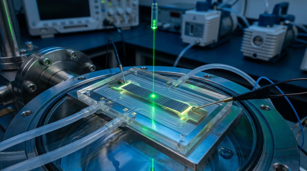
The optical layer involves a focused laser beam directed at the GNR sample. The beam must be focused using a high-numerical-aperture (NA) objective lens to ensure the light intensity is sufficient to trigger the nonlinear optical response at the nanoscale.
The magnetic control layer involves placing the entire sample assembly within the bore of an electromagnet. This allows for the application of a uniform magnetic field perpendicular or parallel to the GNR axis, depending on the desired spin orientation.
The success of the device depends heavily on the quality of the GNRs. You cannot use standard bulk graphene; you must use high-quality nanoribbons with controlled edge states. This requires advanced /blog/category/graphene-production/ techniques.
Step 1: Substrate Preparation
Clean the Si/SiO2 or hBN substrate using a standard RCA cleaning process to remove all organic and ionic contaminants. Any residue will break the BLPH symmetry and introduce unwanted charge currents.
Step 2: GNR Synthesis
The most reliable method for producing semiconducting GNRs is via bottom-up chemical vapor deposition (CVD) using precursor molecules. To create the Janus structure, the precursor molecules must be designed to deposit different functional groups on the top and bottom surfaces of the ribbon. This is a complex chemical process that often requires specialized precursors like substituted polyphenylene derivatives.
Step 3: Transfer and Alignment
If the GNRs are grown on a metal catalyst (like copper or nickel), they must be transferred to the target substrate (Si/SiO2 or hBN) using a polymer-assisted transfer method. During transfer, ensure the ribbons are aligned using optical microscopy or scanning electron microscopy (SEM) to facilitate probe placement.
Step 4: Contact Deposition
Deposit gold or palladium electrodes using electron-beam evaporation. The contacts should be placed at the ends of the GNRs to allow for the measurement of the induced DC currents.
Once the prototype is assembled, follow these steps to demonstrate the generation of pure spin currents.
Step 1: Laser Calibration
Determine the bandgap of your GNRs using UV-Vis spectroscopy. Select a laser wavelength that is slightly higher in energy than the bandgap to ensure efficient excitation of the electronic states responsible for the nonlinear response.
Step 2: Optical Alignment
Position the laser so that the beam is focused directly onto the GNR channel. Use a polarizingizer to control the light's polarization angle. The research suggests that the nonlinear response is highly sensitive to the light's polarization relative to the ribbon's symmetry axes.
Step 3: Magnetic Field Initialization
Apply a small bias magnetic field to stabilize the ferromagnetic order in the Janus GNRs.
Step 4: Data Acquisition
Start with the laser at a low power and slowly increase it. Monitor the voltage at the electrodes. You are looking for a DC voltage that corresponds to the spin-driven current. Because the charge current is suppressed by the BLPH symmetry, the measured voltage should be significantly lower than what would be expected in a non-symmetric ribbon, while the spin-related signal remains robust.
Step 5: Magnetic Field Sweep
Gradually sweep the external magnetic field from negative to positive. As the field changes, the direction of the induced DC spin current should flip, demonstrating the tunability of the device.
Detecting a pure spin current is notoriously difficult because, by definition, there is no net charge flow. However, in a ferromagnetic GNR, the spin current can be converted into a measurable electrical signal through the Inverse Spin Hall Effect (ISHE) or by measuring the voltage generated at the contacts due to the spin-dependent chemical potential.
To implement this in a lab:
1. Use a lock-in amplifier: Since the signal is likely very small, a lock-in amplifier synchronized with the laser pulse frequency is essential to extract the signal from the noise.
2. Differential measurement: Measure the voltage with the magnetic field at zero and then at various field strengths. The difference in voltage provides a clearer picture of the spin current's behavior.
3. Temperature dependence: Perform measurements at varying temperatures. If the effect is truly driven by the BLPH symmetry and the ferromagnetic order, the signal should follow the magnetization curve of the GNR material.
Since this is a cutting-edge application, the following parameters are proposed as cautious starting ranges for a prototype. These are engineering assumptions based on the research and typical GNR behavior.
GNR Width: 5 nm to 15 nm. Wider ribbons may lose the semiconducting properties and the BLPH symmetry constraint.
Laser Power: 1 mW to 50 mW at the sample surface. High power can cause thermal damage, while low power may not trigger the nonlinear response.
Laser Wavelength: 800 nm to 1500 nm (Near-Infrared). This depends on the specific bandgap of the synthesized GNR.
Magnetic Field Strength: 0 to 1 Tesla. Most ferromagnetic GNRs will reach saturation within this range.
Substrate Temperature: 4K to 300K. While room temperature operation is the goal, 4K is recommended for initial validation of the symmetry-driven effects.
There are several technical risks that can lead to failure in this prototyping process.
Risk 1: Symmetry Breaking by Defects
Any structural defect, such as a missing carbon atom or an unintended functional group, will break the bipartite-lattice symmetry. This will lead to a significant increase in charge currents, drowning out the spin current signal.
Mitigation: Use high-resolution TEM (Transmission Electron Microscopy) to verify the structural integrity of the GNRs before proceeding to the measurement stage.
Risk 2: Thermal Noise and Heating
Even though the charge current is suppressed, the absorption of laser energy will cause local heating. This can disrupt the ferromagnetic order or create thermal currents (Seebeck effect).
Mitigation: Use ultra-short (femtosecond) pulses with low duty cycles to minimize heat accumulation. Use a cryogenic stage to sink heat away from the sample.
Risk 3: Substrate Interference
The substrate can introduce its own electronic signals or trap charges that interfere with the GNR's response.
Mitigation: Use hexagonal Boron Nitride (hBN) as a substrate. It is atomically smooth and has minimal electronic interference compared to Si/SiO2.
Risk 4: Contact Resistance
High contact resistance at the metal-GNR interface can prevent the detection of the small induced currents.
Mitigation: Use electron-beam evaporation for contact deposition and consider a post-deposition annealing step to improve the interface quality.
The discovery that bipartite-lattice particle-hole symmetry can suppress charge currents while allowing for tunable spin currents is a game-changer for spintronics. By utilizing ferromagnetic Janus graphene nanoribbons, engineers can create devices that are both highly efficient and easily controlled via external magnetic fields.
While the fabrication and measurement requirements are high—requiring precise CVD growth and sensitive optical detection—the potential for creating ultra-low-power, light-driven spintronic components is immense. For any lab or startup looking to lead in the next era of nanoelectronics, mastering the control of these spin shift currents should be a top priority.
For related commercial context, explore graphene electronics and turbostratic graphene flakes.
Serious about B2B integration? Test our premium Pulsed Electrical Resistive Carbon Heating turbostratic graphene in your lab. 100g sample packs available now.
Explore More
Researchers derived the first exact formula for resistivity in the 1D infinite-U Hubbard model, providing a crucial benchmark for understanding strongly...

Researchers propose a novel method to detect spin- and valley-polarized states in van der Waals materials, a key step for next-gen spintronics and...

Researchers developed the CARBON-2D Topological Descriptor (C2DTD), an interpretable, physics-informed method to rapidly predict the properties of new 2D...