
Physisorbed Metal Nanoparticles: Contact Mechanics on Surfaces
Discover the importance of physisorbed metal nanoparticles and their contact mechanics. This research explores how Al and Cu particles interact on a nanoscale.
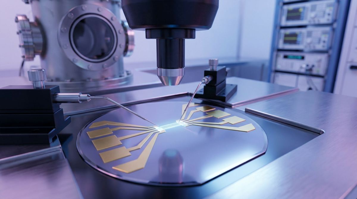
The frontier of quantum computing and ultra-sensitive sensing is built upon a single, fundamental component: the Josephson junction. This device, typically made from two superconductors separated by a thin insulating barrier, allows for the creation of qubits and SQUIDs. The challenge has always been control. Fabricating these junctions is difficult, and tuning their properties after they are made is even harder. Recent breakthroughs in two-dimensional materials, however, are changing the game completely.
A 2026 paper by Philipp Schmidt and his colleagues demonstrates a powerful new platform that combines bilayer graphene with a superconductor, Niobium Diselenide (NbSe₂). They showed that superconductivity can be induced in the graphene over remarkable distances—more than a micrometer—simply by placing it next to the NbSe₂. More importantly, they proved that this induced superconductivity can be precisely controlled using local electrostatic gates. This opens the door to creating Josephson junctions that are not just fabricated, but programmed.
This guide will walk you through the practical steps to translate that foundational research into a functional prototype: a gate-tunable graphene Josephson junction. We will cover the design, materials, fabrication process, and testing plan for a device that could serve as a building block for the next generation of graphene electronics.
Our objective is to build a two-terminal electronic device where a channel of bilayer graphene acts as the "weak link" between two superconducting contacts. The key innovation is that the properties of this graphene link, and therefore the entire junction, can be tuned in real-time by applying voltage to a nearby gate electrode.
In essence, we are building a superconducting switch. By changing the gate voltage, we can modulate the supercurrent flowing through the graphene, effectively turning the junction "on," "off," or setting it to an intermediate state. This level of electrical control is the holy grail for creating complex, scalable quantum circuits. The final device will consist of a channel of high-quality bilayer graphene sandwiched between hexagonal boron nitride (hBN), with NbSe₂ contacts at either end and a set of local metal gates underneath.
This project is directly inspired by the work of Schmidt et al. (arXiv:2609.16320v1). Their research provides the critical proof of concept for our device. While their primary goal was to probe and understand the physics of proximity-induced superconductivity, their platform contains all the necessary elements for our application.
Key takeaways from their work that we will leverage:
1. Proximity Effect: They confirmed that NbSe₂ induces a robust superconducting gap (up to 80 μeV) in adjacent bilayer graphene. This is the core physical phenomenon our device relies on.
2. Long Coherence Length: The superconductivity persisted over a distance of more than one micrometer. This gives us a generous length scale to design our graphene channel, making fabrication more feasible than in systems requiring angstrom-level precision.
3. Gate Control: They used local electrostatic gates to create quantum dots and tunnel barriers within the graphene. We will adapt this technique to use a gate to control the entire channel's carrier density, thereby tuning the Josephson energy and critical current of our junction.
Their paper focuses on using quantum dots as local probes. We will simplify the geometry to create a straightforward two-terminal junction, applying their principles of material combination and gate control to a different end goal.
Building this prototype requires a cleanroom environment and specialized nanofabrication tools. This is not a weekend project, but it is within reach for a university lab, a well-equipped maker space, or a startup focused on quantum hardware.
Materials:
Bilayer Graphene (BLG): High-quality, mechanically exfoliated flakes are required. The electronic properties must be pristine. While exfoliated flakes from kish graphite are the standard for research, companies exploring scalable production might investigate CVD-grown sheets or sources of industrial graphene supply, though performance may differ.
Niobium Diselenide (NbSe₂): Bulk crystals for mechanical exfoliation. This will serve as our superconductor.
Hexagonal Boron Nitride (hBN): High-purity bulk crystals for exfoliation. We need atomically flat flakes to encapsulate the graphene, protecting it from contamination and providing a superior dielectric environment.
Substrate: A silicon wafer with a 285 nm or 300 nm layer of thermally grown silicon dioxide (Si/SiO₂). The silicon acts as a global back gate.
Metal Targets: High-purity chromium (Cr) and gold (Au) for fabricating the gate electrodes and normal metal contacts.
Equipment:
Glovebox: An inert atmosphere (argon or nitrogen) is crucial for assembling the material stack to prevent contamination.
Mechanical Exfoliation Setup: High-quality adhesive tape (e.g., Nitto tape) and optical microscopes for finding and identifying suitable flakes of graphene, hBN, and NbSe₂.
Van der Waals Heterostructure Transfer Station: A high-precision XYZ stage with rotation, heating, and microscope optics for picking up and stacking the 2D material flakes.
Electron-Beam Lithography (EBL) System: For patterning nanoscale features like the local gates and contact areas.
Reactive Ion Etcher (RIE): A plasma etcher (e.g., using CHF₃/O₂) to shape the graphene channel.
Metal Evaporator: An e-beam or thermal evaporator for depositing the Cr/Au gate electrodes.
Atomic Force Microscope (AFM): Essential for verifying flake thickness, checking for surface contamination, and confirming device geometry post-fabrication.
Cryostat: A dilution refrigerator or ³He system capable of reaching millikelvin temperatures is necessary to perform the superconducting measurements.
Measurement Electronics: Low-noise voltage/current sources, nanovoltmeters, and lock-in amplifiers.
The fabrication process involves multiple stages of lithography, material transfer, and deposition. Meticulous care and cleanliness are paramount at every step.
Step 1: Local Gate Fabrication
1. Start with a clean Si/SiO₂ substrate.
2. Use EBL to define the pattern for your local gate electrodes. For a simple junction, a single gate electrode running underneath the future graphene channel is sufficient.
3. Engineering Assumption: The source paper uses complex gate geometries to define quantum dots. For our junction, a single gate with a width of 50-100 nm is a good starting point.
4. Deposit 5 nm of Cr (as an adhesion layer) followed by 20-30 nm of Au using an e-beam evaporator.
5. Perform liftoff in a solvent (e.g., acetone) to leave only the patterned metal gates on the substrate.
Step 2: Van der Waals Stack Assembly
This is the most delicate part of the process and should be performed in a glovebox.
1. Exfoliate hBN, BLG, and NbSe₂ onto separate Si/SiO₂ chips.
2. Using an optical microscope, identify suitable flakes. You will need a large, clean bottom hBN flake, a uniform BLG flake, a smaller top hBN flake, and two NbSe₂ flakes for the contacts. Use AFM to confirm the BLG is indeed a bilayer (~0.7 nm thick).
3. Use the transfer station to assemble the stack. First, pick up the top hBN flake. Then, use it to pick up the BLG flake. Finally, pick up the two NbSe₂ flakes, positioning them at what will be the ends of your channel.
4. Engineering Assumption: The source paper places the NbSe₂ laterally after the stack is placed. An alternative, and perhaps simpler, method is to pick up the NbSe₂ flakes with the stamp first, then pick up the hBN/graphene stack to place on top of them. However, the lateral contact method from the paper likely produces a cleaner interface. For this guide, we will follow the paper's implicit lateral contact geometry.
Step 3: Stack Transfer and Channel Definition
1. Carefully align your assembled stack over the pre-patterned local gates on your device substrate and place it down. Heat the substrate gently (around 50-70 °C) to promote adhesion and release the stack from the transfer polymer.
2. Use EBL to pattern a resist mask that defines the final shape of your graphene channel. This mask should protect a rectangular or Hall bar shape that connects the areas where the superconducting contacts will be.
3. Use a gentle RIE plasma etch to remove the unprotected graphene.
4. Remove the resist mask. You now have an encapsulated graphene channel sitting directly above your local gate.
Step 4: Contact Deposition
1. Use a final EBL step to open windows in a resist layer over the ends of the graphene channel and the NbSe₂ flakes.
2. Immediately before loading into the evaporator, perform a short Argon plasma clean to remove any polymer residue from the contact areas. This is critical for good electrical contact.
3. Deposit the superconducting contacts. The source paper uses lateral proximity, so we will deposit Cr/Au (e.g., 5 nm / 80 nm) that overlaps both the edge of the graphene channel and the pre-placed NbSe₂ flakes. This bridges the superconductor to the graphene.
4. Perform liftoff to finalize the device.
The final device has a simple architecture. A current is passed through the two superconducting contacts, flowing through the graphene channel. The voltage drop across the channel is measured. The local gate sits directly below the graphene, separated by the thin bottom hBN flake.
Operation is straightforward:
1. The device is cooled down below the critical temperature of NbSe₂ (~7 K) and the proximity-induced gap in the graphene (which requires millikelvin temperatures to observe clearly).
2. Without any gate voltage applied (V_g = 0), the graphene channel becomes superconducting due to the proximity effect. When you sweep a current (I_sd) through the device, you should measure zero voltage (V_sd = 0) up to a certain critical current (I_c). Above I_c, the superconductivity breaks down, and a finite voltage appears.
3. By applying a voltage to the local gate (V_g), you change the number of charge carriers (electrons or holes) in the graphene. This change in carrier density directly affects the ability of Cooper pairs to transit the channel, thus modulating the critical current I_c. A positive V_g will add electrons, while a negative V_g will add holes. Sweeping V_g allows you to tune I_c from its maximum value down to zero, effectively turning the junction off.
This gate tunability is the key feature, transforming a static component into a dynamic one, essential for building complex graphene applications.
Verifying the device's performance requires cryogenic measurements.
1. Room Temperature Checks: Before cooling down, perform basic two-terminal resistance measurements on all contacts to check for continuity. Measure the resistance between the gate and the channel to ensure there is no gate leakage. A high resistance (>1 GΩ) is expected.
2. Cooldown and Initial I-V Curve: Cool the device in a dilution refrigerator. At base temperature (e.g., <100 mK), perform a DC current-voltage (I-V) measurement. Sweep the source-drain current I_sd from negative to positive and measure V_sd. You are looking for a distinct "superconducting branch" around zero current where V_sd remains zero. The current at which a voltage suddenly appears is the critical current, I_c.
3. Gate Modulation: Park the device at a specific gate voltage, V_g, and measure the I-V curve to find I_c. Repeat this for a wide range of V_g values. Plot I_c as a function of V_g. You should see a clear modulation, demonstrating that you can control the junction with the gate. The device will likely show ambipolar behavior, with superconductivity being suppressed near the charge neutrality point of the graphene.
4. Magnetic Field Response: A definitive test for a Josephson junction is its response to a magnetic field applied perpendicular to the device plane. Measure I_c as a function of the magnetic field (B). The resulting plot should show a Fraunhofer pattern—a central peak with decaying side lobes, similar to a sinc function. This pattern is a textbook signature of a uniform Josephson junction.
This is a cutting-edge project, and success is not guaranteed. It is important to be aware of the assumptions and risks.
Assumptions:
Channel Dimensions: The source paper reports effects over 1 μm. We will assume a channel length of 500 nm and a width of 1-2 μm as a good starting point. These dimensions are achievable with EBL and offer a good balance between signal strength and gate control.
Interface Quality: We assume that the van der Waals assembly process will yield a clean, electronically transparent interface between the NbSe₂ and the graphene. Any contamination or bubbles at this interface will severely degrade or completely destroy the proximity effect.
Material Quality: This guide assumes access to high-purity, single-crystal 2D materials. The long-range proximity effect observed in the source paper is a direct result of the highly ballistic (low-disorder) nature of their encapsulated bilayer graphene. Lower-quality materials will not work.
Risks:
Fabrication Yield: Nanofabrication of 2D material heterostructures has a notoriously low yield. Flakes can be contaminated, stacks can have bubbles, and lithography steps can fail. Expect to fabricate multiple devices to get one that works.
Contact Resistance: Achieving a low-resistance contact between a 3D metal and a 2D material is a persistent challenge. The Argon cleaning step is critical but can also damage the graphene if too aggressive.
Cryogenic Failures: Wires can break, and devices can be destroyed by electrostatic discharge during handling and cooling. Proper ESD protection and careful wiring are essential.
Successfully building and testing a gate-tunable graphene Josephson junction is a significant achievement. It is a foundational step toward more complex quantum devices. A single junction is a switch; two junctions in a loop create a SQUID, the most sensitive magnetic field detector known. An array of such junctions, individually controlled by local gates, forms the basis of a programmable quantum processor.
The platform demonstrated by Schmidt et al. and adapted in this guide offers a pathway to scalable quantum hardware. Unlike traditional junctions that are fixed at the time of fabrication, these graphene-based devices can be tuned, reconfigured, and coupled on-demand using simple voltages. This electrical control, combined with the material advantages of graphene, positions this technology as a leading candidate for the future of quantum information and sensing. The journey from a single prototype to a full-scale processor is long, but the fundamental building block is now within reach.
Serious about B2B integration? Test our premium Pulsed Electrical Resistive Carbon Heating turbostratic graphene in your lab. 100g sample packs available now.
Explore More
Discover the importance of physisorbed metal nanoparticles and their contact mechanics. This research explores how Al and Cu particles interact on a nanoscale.

Researchers explore interaction-driven transport in graphene, where massless Dirac fermions can drag massive particles, creating a current without direct...

Researchers have developed a high-efficiency graphene-silicon microring modulator, a critical step toward faster, lower-power optical communications and...