
Graphene-Silicon Modulator Unlocks High-Efficiency Optical Switching at Key
Researchers have developed a high-efficiency graphene-silicon microring modulator, a critical step toward faster, lower-power optical communications and...
Graphene nanoribbons (GNRs), which are narrow strips of single-layer graphene, represent a frontier in materials science. Unlike their two-dimensional parent, GNRs can have a significant electronic band gap, making them suitable for semiconductor applications. The challenge has always been precision. The properties of a GNR are exquisitely sensitive to its width, edge structure (armchair or zigzag), and any chemical modifications. For years, this sensitivity was a liability, leading to inconsistent materials. Today, advances in bottom-up synthesis are turning it into an asset, allowing for the creation of GNRs with atomically precise, custom-designed properties.
This guide is based on recent computational research that characterizes a highly specific, synthesized GNR. This material, a nine-atom-wide armchair GNR with periodic pores and pyrazinic nitrogen doping, has electronic and optical properties that are deliberately engineered at the atomic level. The research shows that this structure has a tailored band gap and a strong response to light in the red and near-infrared part of the spectrum.
Here, we translate these research findings into a practical engineering project: building a prototype narrowband photodetector. This device will leverage the unique properties of these designer GNRs to selectively detect light of a specific color. This project is ambitious and suited for a small lab, university research group, or a startup with access to basic fabrication facilities. We will walk through the device concept, required materials, a step-by-step prototyping plan, and a testing protocol to validate your build. This exploration into advanced materials showcases the growing list of real-world graphene applications.
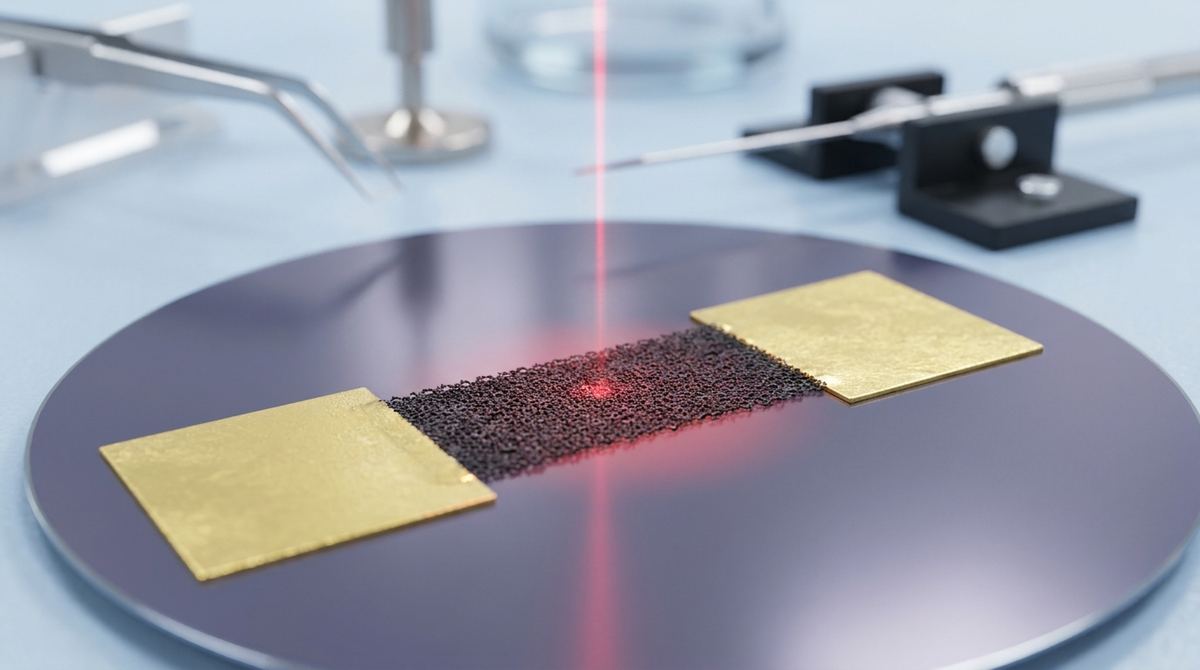
We aim to build a two-terminal photoconductive device. The concept is straightforward: a single or an array of these specialized GNRs will bridge two metal electrodes on an insulating substrate. In its resting state (in the dark), the GNR has a certain electrical resistance. When illuminated with photons of the correct energy, the GNR absorbs the light, generating electron-hole pairs (excitons). These charge carriers increase the material's conductivity, causing a measurable drop in resistance.
The key innovation here comes from the material itself. The research by de Araújo et al. (2026) shows that the combination of periodic pores and nitrogen doping in this specific GNR does two crucial things. First, it opens the band gap to a useful range. Second, the nitrogen atoms shift the absorption edge into the red and create strongly bound excitons. This means the material is most sensitive to a specific range of lower-energy light.
Our goal is to build a device that exhibits a peak photoresponse at this engineered wavelength. Such a device could be useful in applications requiring narrowband light detection without the need for external filters, such as specialized optical communication systems, chemical sensing, or certain types of imaging. The field of graphene sensors is rapidly expanding, and this prototype represents a step toward highly selective optical detectors.
Successfully building this prototype requires access to highly specialized materials and standard microfabrication equipment.
1. Active Material: Pyrazinic Nitrogen-Doped Porous 9-AGNRs. This is the heart of the device and the most challenging component to acquire. The source paper describes its synthesis via a bottom-up, on-surface method using a phenazine-bearing precursor molecule on a metallic surface.
- Sourcing Assumption: Acquiring this exact GNR is a significant hurdle. Options include:
- Attempting the on-surface synthesis in-house if you have an ultra-high vacuum (UHV) system. This is a complex process detailed in surface science literature.
- Collaborating with a research institution that specializes in GNR synthesis.
- Purchasing from a specialty chemical or materials science supplier, though availability of this specific GNR is not yet widespread. You may need to commission a custom synthesis.
2. Substrate: A 300 nm layer of silicon dioxide (SiO2) on a doped silicon wafer (Si). This is a standard platform for nanoelectronics. The doped Si layer can serve as a back gate to tune the GNR's electronic properties, while the SiO2 provides electrical insulation.
3. Electrodes: High-purity gold (Au) with a thin chromium (Cr) or titanium (Ti) adhesion layer. Palladium (Pd) is also an excellent contact material for graphene.
4. Encapsulation (Recommended): Hexagonal boron nitride (h-BN) flakes. High-quality h-BN can protect the GNR from atmospheric contaminants and improve device performance by providing a clean, flat interface.
1. Fabrication:
- Electron Beam Lithography (EBL) or Photolithography system for patterning electrodes.
- Electron Beam or Thermal Evaporator for metal deposition.
- Reactive Ion Etcher (RIE) for substrate cleaning or patterning (optional).
- Spin Coater for applying polymer resists.
2. Material Handling and Transfer:
- Glovebox or vacuum chamber for handling air-sensitive materials.
- Microscope with manipulators for the transfer of GNRs and h-BN flakes.
3. Characterization and Testing:
- Atomic Force Microscope (AFM) to verify GNR transfer and device integrity.
- Raman Spectrometer to confirm the structural quality of the GNR.
- Semiconductor Parameter Analyzer or Source-Measure Unit (SMU).
- Probe Station for making electrical contact with the device.
- Tunable light source: A monochromated white light source or a set of lasers with different wavelengths covering the visible to near-infrared spectrum.
- Optical power meter to calibrate the incident light intensity.
This section outlines the major steps to fabricate the photodetector. We will assume you have successfully sourced the GNRs, which are likely synthesized on a metal foil like gold or copper.
The as-synthesized GNRs must be moved from their growth substrate to the target SiO2/Si wafer. A common method is the polymer-assisted wet transfer.
1. Coat the Growth Substrate: Spin-coat a layer of a support polymer, such as polymethyl methacrylate (PMMA), over the GNRs on their original metal foil.
2. Etch the Metal: Float the PMMA-coated foil on a chemical etchant that will dissolve the metal but not the GNRs or PMMA. For a gold substrate, a potassium iodide/iodine solution can be used. For copper, ammonium persulfate or ferric chloride is common. This will leave you with a floating PMMA/GNR film.
3. Rinse: Carefully transfer the floating film to several baths of deionized water to remove residual etchant.
4. Scoop and Dry: Scoop the cleaned film out of the water using your target SiO2/Si wafer. Let it dry slowly in a controlled environment to ensure good adhesion.
5. Remove the Polymer: Bake the wafer on a hotplate at a moderate temperature (e.g., 180 °C) to improve adhesion and then dissolve the PMMA support layer using a solvent like acetone, followed by an isopropyl alcohol rinse.
Engineering Assumption: This transfer process is a standard but delicate procedure. The source paper notes that the GNRs have a weak van der Waals interaction with metal substrates, which is a positive indicator that they can be lifted off without significant damage to their intrinsic properties.
After transfer, you will have randomly dispersed GNRs on your wafer.
1. Locate: Use an optical microscope and, more importantly, an AFM to locate suitable GNRs or small patches of aligned GNRs. You are looking for long, clean ribbons.
2. Design: Based on the AFM map, design the electrode pattern using CAD software. The electrodes should overlap the ends of the GNR. A typical channel length (the gap between electrodes spanned by the GNR) could be anywhere from 100 nm to a few micrometers.
This step uses lithography to create the electrical connections to your GNR.
1. Apply Resist: Spin-coat the appropriate resist (e.g., EBL resist) over the entire substrate, covering the GNR.
2. Pattern: Use the EBL system to write the electrode pattern into the resist, exposing the areas where the metal should be.
3. Develop: Submerge the wafer in a developer solution to remove the exposed resist, creating a stencil for metal deposition.
4. Deposit Metal: Place the wafer in an evaporator and deposit the adhesion layer (e.g., 5 nm of Cr) followed by the contact metal (e.g., 50-100 nm of Au).
5. Lift-Off: Submerge the wafer in a solvent (e.g., acetone) to dissolve the remaining resist. This will lift off the unwanted metal, leaving only your patterned electrodes making contact with the GNR.
The precise control required for these fabrication steps is a core topic in graphene electronics and photonics.
To protect the device and improve performance, you can encapsulate it with an h-BN flake. This is done using a dry transfer technique, which involves picking up a thin h-BN flake with a special polymer stamp and carefully placing it over the GNR device. This is an advanced technique that requires practice.
With the device fabricated, you need to test its electrical and optical properties to see if it functions as a photodetector.
First, measure the device in complete darkness to understand its fundamental electronic behavior.
- Connect the device to the SMU using the probe station.
- Perform a two-terminal voltage sweep (e.g., from -1 V to +1 V) and measure the resulting current. This gives you the dark I-V curve.
- From this curve, you can calculate the device's dark resistance. A high resistance is expected, as the GNR is a semiconductor.
- If you included a back gate, you can also measure the I-V curve at different gate voltages to see if you can modulate the GNR's conductivity (the field effect).
Now, test the device's response to light.
- Position the device under your tunable light source. Ensure the light spot is focused on the GNR between the electrodes.
- Set the light source to a specific wavelength, starting in the near-infrared and moving toward the visible spectrum.
- Measure the I-V curve while the device is illuminated. You should observe a higher current (lower resistance) compared to the dark measurement. The difference, I_photo = I_light - I_dark, is the photocurrent.
- Repeat this measurement for a range of wavelengths. It is critical to keep the incident optical power constant across all wavelengths. Use your power meter to calibrate the source at each step.
- Plot Photocurrent vs. Wavelength: The resulting graph is the photoresponse spectrum of your device. Based on the source paper, you should expect to see a peak in the red or near-infrared region, corresponding to the GNR's primary absorption feature.
- Calculate Responsivity (R): This is a key metric for a photodetector. It is the photocurrent generated per unit of incident optical power. R = I_photo / P_incident. Calculate this at the peak response wavelength.
- Estimate Rise and Fall Times: By pulsing the light source on and off with a modulator and measuring the current response over time with an oscilloscope, you can determine how quickly your detector responds.
This is a challenging project with a high risk of failure, typical of cutting-edge materials research.
- Risk: Material Availability. As discussed, sourcing these specific GNRs is the primary obstacle.
- Mitigation: The most practical approach is academic or industrial collaboration. The processes involved in graphene manufacturing techniques for such precise structures are not yet trivial.
- Risk: Process-Induced Damage. The GNRs are fragile. The transfer and fabrication steps can easily damage or contaminate them.
- Mitigation: Extreme care and cleanliness are paramount. Work in a cleanroom environment. Use AFM imaging after each major step to inspect for damage. Fabricate an array of devices on the same chip to increase the probability of getting a few working ones.
- Risk: High Contact Resistance. A poor connection between the metal electrodes and the GNR can dominate the device's resistance, masking the true photoresponse.
- Mitigation: Choose contact metals known to work well with graphene (Pd, Au). Consider a gentle thermal anneal after fabrication (e.g., in a vacuum or forming gas environment) to improve the contact interface.
- Risk: No Measurable Photoresponse. The signal may be too small to detect.
- Mitigation: Ensure your measurement setup has low noise. Use a lock-in amplifier with a chopped light source to detect very small signals. Try applying a gate voltage to tune the GNR into a more responsive state.
This practical guide is a direct engineering interpretation of the findings presented by de Araújo et al. (2026).
- Source: The paper computationally demonstrates that pyrazinic nitrogen doping in a porous 9-AGNR selectively narrows the conduction band and red-shifts the optical absorption edge.
- Our Interpretation: This specific electronic structure is ideal for a narrowband photodetector operating at lower energies (red/NIR).
- Source: The research shows a very large exciton binding energy of 414 meV.
- Our Interpretation: This is highly beneficial for a photodetector. It means that when a photon is absorbed, the resulting electron-hole pair is tightly bound and less likely to immediately recombine without contributing to the photocurrent, potentially leading to higher device efficiency.
- Source: The paper confirms that the GNRs interact weakly (via van der Waals forces) with common metal substrates like Au(111).
- Our Interpretation: This supports the feasibility of the polymer-assisted transfer process, as the GNRs are not chemically bonded to their growth substrate and can be lifted off.
All other details, including the specific device layout, the use of a SiO2/Si substrate, the transfer and lithography methods, and the testing parameters, are engineering assumptions based on established best practices in the field of 2D material device fabrication.
Serious about B2B integration? Test our premium Pulsed Electrical Resistive Carbon Heating turbostratic graphene in your lab. 100g sample packs available now.
Explore More
Researchers have developed a high-efficiency graphene-silicon microring modulator, a critical step toward faster, lower-power optical communications and...

Discover how preempted band-inversion transitions in graphene-based systems create a self-doped crystal, a revolutionary material for ultra-clean electronics.

Discover how strain-induced curvature in monolayer graphene can engineer its electronic bandgap and thermal conductivity for next-generation flexible...