
Practical Guide: Prototyping a Graphene Nanoribbon Photodetector
Build a near-infrared photodetector with nitrogen-doped porous graphene nanoribbons. This guide details the materials, fabrication steps, and test plan.
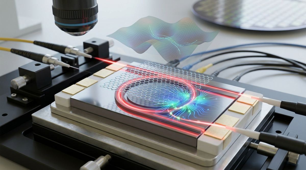
The insatiable demand for faster data transmission, from global internet backbones to the processors inside a single data center, is pushing our current electronic technologies to their physical limits. The wires connecting our world are getting crowded. The solution, for decades, has been to replace electrons with photons, using light to carry information through fiber optic cables. Now, the challenge is to bring this light-based communication, known as photonics, directly onto the silicon chips that power our computers. The goal is to create optical interconnects that are faster, smaller, and vastly more energy-efficient than their copper-wire counterparts. A key component for this vision is the optical modulator, a tiny switch that encodes data onto a beam of light. Recent work in this area has produced a particularly promising design that cleverly combines the strengths of traditional silicon with the extraordinary properties of graphene.
At the heart of optical communications is the need to control light rapidly and efficiently. A modulator acts as a gate, turning a steady beam of light into a flashing signal that represents digital ones and zeros. For this to work on a silicon chip, the modulator must be incredibly small, switch on and off billions or even trillions of times per second, and consume very little power. While silicon is a fantastic material for guiding light, it is notoriously bad at modulating it. Modifying silicon’s optical properties requires large, power-hungry devices that are difficult to integrate into compact circuits. Engineers have devised clever tricks to make silicon modulators work, but they often represent a compromise between size, speed, and power consumption. This bottleneck limits the potential of on-chip photonics. The search is on for a new material that can be seamlessly integrated with the mature silicon fabrication industry but offers superior electro-optical performance. This is the challenge that a team of researchers, including Chao Luan, Deming Kong, Yong Liu, Yunhong Ding, and Hao Hu, has addressed by turning to the unique potential of a one-atom-thick sheet of carbon: graphene.
The central innovation in this research is the fusion of three distinct technologies into one highly effective device. First, the researchers use a standard silicon platform to guide light. Second, they etch this silicon into a microscopic racetrack, called a microring resonator. When light of a specific wavelength passes by this ring, it gets captured and circulates inside it many times, dramatically amplifying its interaction with the waveguide material. Third, and most critically, they integrate graphene into the system in a very specific way. Instead of a solid silicon waveguide, they use a "slot waveguide," which has a minuscule gap running down its center. This gap is where the magic happens. The optical energy of the light is squeezed and concentrated into this tiny slot. By placing a layer of graphene over this slot and applying a small voltage, the researchers can effectively turn the graphene's light absorption on and off. Because the light in the microring is already amplified and the light in the slot is intensely focused, even a tiny change in the graphene has a massive effect on the light passing through the device. This creates an optical switch that is compact, requires very little power, and can operate over a broad range of light frequencies.
To understand the elegance of this design, we must look at each component. The foundation is silicon-on-insulator (SOI), the workhorse platform of modern photonics. Light is confined within a thin layer of silicon that sits atop a layer of silicon dioxide. This structure acts like a microscopic fiber optic cable etched onto a chip.
The first key structure is the microring resonator. This is a closed loop of silicon waveguide placed very close to a straight "bus" waveguide that carries the input and output light. Light traveling down the bus waveguide can hop over into the ring, but only if its wavelength perfectly matches the resonant condition of the ring, which is determined by its circumference. Once inside, the light circulates, creating a high-intensity optical field. This resonant behavior is extremely sensitive; any small disturbance inside the ring can dramatically alter its properties.
The second key structure is the slot waveguide that makes up the ring. Instead of a solid strip of silicon, the waveguide consists of two parallel silicon "rails" separated by a nanometer-scale gap. Due to the physics of electromagnetic fields at boundaries, the light's electric field is powerfully concentrated within this low-refractive-index slot. This is counter-intuitive but incredibly useful, as it allows for unprecedented interaction with any material placed inside that gap.
This is where graphene enters the picture. The device is constructed with a capacitor-like structure, using two layers of graphene separated by a thin insulator, or one layer of graphene and doped silicon. This graphene "capacitor" is placed directly over the slot. Graphene's electronic properties are governed by a unique feature called the Dirac cone, which means it has no bandgap. This allows it to absorb photons over an incredibly wide range of energies. Crucially, this absorption can be controlled with an electric field. By applying a voltage, one can change the "Fermi level" in the graphene, effectively flooding it with charge carriers. This process, known as Pauli blocking, prevents the graphene from being able to absorb photons of a certain energy. In essence, applying a voltage can make the graphene transparent to the light circulating in the ring.
When no voltage is applied, the graphene is absorptive. It acts like a drag on the light circulating in the ring, damping the resonance. As a result, light in the bus waveguide doesn't couple to the ring efficiently and passes straight through to the output. This is the "ON" state. When a voltage is applied, the graphene becomes transparent. The ring can now sustain a strong resonance, capturing light from the bus waveguide and preventing it from reaching the output. This is the "OFF" state. By switching the voltage, the device modulates the light, creating the digital signal. This mechanism is what enables such high-performance graphene electronics.
The title of the paper highlights "high-efficiency," which in the context of an optical modulator refers to a combination of desirable performance metrics. While the source abstract is brief, the design itself points toward several key achievements. First, the efficiency likely refers to a high modulation depth, meaning a very strong contrast between the ON and OFF states. The combination of the microring's resonant enhancement and the slot waveguide's field confinement multiplies the effect of the graphene, leading to a much clearer signal.
Second, high efficiency implies low power consumption. Because the active region is so small and the interaction is so strong, only a very small voltage change is needed to switch the device. This is a critical factor for large-scale systems like data centers, where millions of such components could be operating simultaneously and energy costs are a major concern.
Third, the device operates across two important wavelength bands: 1.5 μm and 2 μm. The 1.5 μm (specifically 1550 nm) region is the backbone of modern telecommunications. The 2 μm band is an emerging frontier for applications like LiDAR for autonomous vehicles, medical diagnostics, and environmental gas sensing. Graphene's inherent broadband absorption capability is what allows a single device architecture to work effectively in both of these distinct spectral windows, demonstrating remarkable versatility that is difficult to achieve with conventional materials.
This research represents a significant step forward in the development of next-generation photonic integrated circuits. By creating a modulator that is small, fast, power-efficient, and broadband, this work addresses several of the primary challenges holding back the widespread adoption of on-chip optical interconnects. In the near term, technologies like this could revolutionize data centers. Replacing electrical wiring between server racks and even between chips with optical links could drastically reduce power consumption and cooling requirements while simultaneously increasing data throughput.
Beyond data centers, this technology opens doors to more advanced and compact sensing systems. A chip-scale spectrometer operating in the 2 μm band could be integrated into a smartphone for health monitoring or into a drone for agricultural analysis. High-efficiency modulators are also essential components for building the complex optical circuits needed for LiDAR systems, which are critical for autonomous navigation. The ability to mass-produce such high-performance optical components on silicon wafers promises to lower costs and increase accessibility, potentially driving innovation across numerous industries. The progress shown here could influence future commercial graphene forecasts for the photonics sector.
While the results suggested by this device architecture are extremely promising, it is important to recognize that this is a research-stage demonstration. Several hurdles must be overcome before such a device can be commercialized. A primary challenge is the manufacturing and integration of high-quality graphene at an industrial scale. The performance of the modulator is directly tied to the purity and uniformity of the graphene layer. Any defects or impurities can scatter light and degrade efficiency. Developing reliable, repeatable processes for growing and transferring large-area, single-crystal graphene onto silicon wafers is an area of intense research and a key focus of advanced graphene manufacturing techniques.
Furthermore, long-term reliability and stability need to be thoroughly investigated. The device must be able to withstand millions of operating cycles over many years without degradation. Environmental factors, such as temperature fluctuations and humidity, could also affect performance, and robust packaging solutions would be required for real-world deployment. Finally, while the design is compatible with silicon manufacturing, the entire process must be optimized to ensure high yields and low costs, which is a non-trivial engineering challenge.
The potential applications for a high-efficiency graphene-silicon modulator are vast and transformative. The most immediate impact would be in high-speed optical transceivers for telecommunications and data communications. These components could enable faster internet speeds and help manage the exponential growth of global data traffic.
In the field of computing, this technology could enable optical I/O (input/output) for microprocessors, breaking the so-called "memory wall" by allowing chips to communicate with memory and with each other at the speed of light. This could lead to a new paradigm in high-performance computing and artificial intelligence hardware.
For sensing, the dual-band operation is particularly exciting. Compact LiDAR systems using 2 μm light would be safer for the human eye and perform better in foggy or hazy conditions. On-chip spectroscopic sensors could be developed for real-time chemical and biological analysis, with applications ranging from industrial process control to point-of-care medical testing. The platform's versatility could even extend to fields like quantum information processing, where precise control of photons is paramount.
If you take away just one idea from this work, let it be this: by strategically placing an electrically tunable, one-atom-thick layer of graphene into a microscopic light-trapping structure on a silicon chip, researchers have created a powerful and highly efficient optical switch. This elegant combination of materials and design principles provides a compelling pathway to building the next generation of technologies that will move and process information using light.
What is an optical modulator?
An optical modulator is a device that encodes an electrical signal onto a beam of light. It acts like a very fast shutter or switch, altering a property of the light, such as its intensity or phase, in response to a changing voltage. This process is fundamental to converting digital electronic data (ones and zeros) into an optical signal that can be sent down a fiber optic cable.
Why is graphene so special for this application?
Graphene has a unique combination of properties that make it ideal for optical modulation. Its two-dimensional nature allows for easy integration onto chip surfaces. Its electronic structure allows it to absorb light over an extremely broad range of wavelengths, and most importantly, this absorption can be dramatically tuned with a small applied voltage. This "electro-absorptive" effect is much stronger in graphene than in many other materials, enabling smaller and more power-efficient devices.
What is a microring resonator?
A microring resonator is a tiny loop of waveguide, typically a few micrometers in diameter, etched onto a chip. When light of a specific wavelength passes near the ring, it couples into it and circulates many times. This process enhances the light's interaction with the material of the waveguide, making the device very sensitive to small changes. It acts as a natural amplifier for the modulation effect.
Why are the 1.5 μm and 2 μm wavelength bands important?
The 1.5 micrometer (1550 nm) band is the primary window used for long-distance fiber optic communications because glass fibers have the lowest signal loss at this wavelength. The 2 micrometer band is an emerging area with significant applications in sensing, LiDAR, and medicine, partly because light at this wavelength is absorbed by specific molecules like water and certain gases, and it is considered more "eye-safe" at higher powers than 1.5 μm light.
Is this technology ready to be used in commercial products?
No, not yet. This work represents a successful proof-of-concept at the research and development stage. Significant engineering challenges remain in terms of large-scale manufacturing, ensuring long-term reliability, and integrating the devices into a complete system. However, it is a crucial and promising step that demonstrates a viable path toward future commercialization.
The work on this high-efficiency graphene-silicon slot-waveguide microring modulator showcases the power of hybrid photonic platforms. By moving beyond monolithic material systems and instead combining the best of what different materials have to offer—the mature fabrication ecosystem of silicon and the unparalleled electro-optical properties of graphene—researchers are paving the way for a new generation of photonic devices. This research provides a clear and compelling blueprint for compact, low-power, and broadband optical switches that could become the building blocks for the future of communications, computing, and sensing. While challenges remain on the path to commercialization, this advancement brings that light-speed future one step closer to reality.
Serious about B2B integration? Test our premium Pulsed Electrical Resistive Carbon Heating turbostratic graphene in your lab. 100g sample packs available now.
Explore More
Build a near-infrared photodetector with nitrogen-doped porous graphene nanoribbons. This guide details the materials, fabrication steps, and test plan.

Discover how preempted band-inversion transitions in graphene-based systems create a self-doped crystal, a revolutionary material for ultra-clean electronics.

Discover how strain-induced curvature in monolayer graphene can engineer its electronic bandgap and thermal conductivity for next-generation flexible...