
How Bending Graphene Unlocks New Electronic and Thermal Properties
Discover how strain-induced curvature in monolayer graphene can engineer its electronic bandgap and thermal conductivity for next-generation flexible...
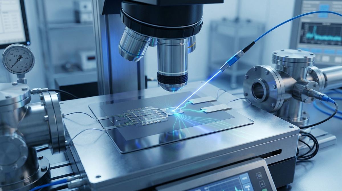
Spintronics, or spin electronics, represents a paradigm shift from conventional electronics. Instead of just using the charge of an electron, spintronics also leverages its intrinsic spin, a quantum mechanical property. This additional degree of freedom promises devices that are faster, smaller, and more energy-efficient. A central challenge in spintronics, however, is the efficient conversion of spin information into a measurable electrical signal. This process, known as spin-to-charge conversion, is the bridge between the quantum world of spin and the classical world of electrical current.
A recent theoretical paper by David T. S. Perkins and Joseph J. Betouras, "Pressure and Proximity Tuned Twisted Bilayer Graphene," outlines a fascinating new approach to this problem. Their work suggests that a carefully constructed stack of two-dimensional materials can create a highly efficient and, more importantly, a tunable spin-to-charge converter. The system involves twisted bilayer graphene (tBLG) encapsulated by a transition metal dichalcogenide (TMD). The key insight is that applying uniaxial pressure to this structure can precisely control its electronic and spintronic properties.
This guide translates that theoretical framework into a practical project for an advanced amateur, university lab, or R&D startup. We will outline the steps to fabricate and test a prototype device that demonstrates pressure-tunable spin-to-charge conversion via the Edelstein effect. This project explores the cutting edge of graphene electronics and could serve as a building block for future spintronic sensors, memory, or logic devices.
The objective is to build a device that converts an injected spin current into a transverse charge current. The defining feature of this prototype is an external control knob: mechanical pressure. By applying controlled, uniaxial strain to the device, we aim to modify the conversion efficiency in a predictable and repeatable manner.
The device will be based on a Hall bar geometry, a standard structure for studying transport phenomena in materials. Spin-polarized electrons will be injected at one end, and the resulting charge current will be measured across the device. A piezoelectric actuator or a similar mechanism will be integrated into the experimental setup to apply pressure.
Success for this project is defined by observing a clear correlation between the applied pressure and the magnitude of the measured output charge current, demonstrating that the spintronic properties of the graphene heterostructure can be mechanically tuned. This provides a physical proof-of-concept for the theoretical predictions in the source paper.
This guide is based on the theoretical findings of Perkins and Betouras (arXiv:2609.20958v1). It is crucial to understand that their paper presents a computational and theoretical model, not an experimental realization. Therefore, this guide involves making several engineering assumptions to bridge the gap between theory and a physical prototype.
What we take from the source:
1. The core device architecture: Twisted bilayer graphene encapsulated by a TMD.
2. The physical mechanism: The proximity effect from the TMD induces strong spin-orbit coupling in the graphene, enabling the Edelstein effect (spin-to-charge conversion).
3. The tuning method: Uniaxial pressure alters the band structure and Berry curvature of the system, which in turn modifies the efficiency of the spin-to-charge conversion.
4. The key advantage: The model predicts a purely collinear Edelstein effect, meaning the output charge current flows in a straight, predictable direction relative to the injected spin polarization, which simplifies device design and improves signal integrity.
Our engineering assumptions:
1. Material Selection: The paper does not specify a particular TMD. We will assume Tungsten Diselenide (WSe2) is a suitable choice due to its well-documented strong spin-orbit coupling. We will use hexagonal boron nitride (hBN) as the encapsulating dielectric for its atomically flat surface and insulating properties.
2. Fabrication Method: We will outline a process based on mechanical exfoliation and dry-stacking, a common technique in academic labs for creating high-quality van der Waals heterostructures.
3. Device Geometry: A standard Hall bar geometry will be used for ease of measurement, though other geometries could be explored.
4. Parameter Ranges: The paper does not provide specific values for twist angle, pressure levels, or operating temperatures. We will propose cautious starting points. For the twist angle, while the "magic angle" of ~1.1 degrees is famous for superconductivity, the effects described are more general. We will target an angle in the range of 1-2 degrees. Pressure will be applied in the GPa range, as is common for tuning 2D materials, but starting with lower, calibrated pressures is essential. Measurements will be planned for cryogenic temperatures to reduce thermal noise.
Fabricating a device at this level requires specialized materials and equipment common in a nanofabrication facility or a well-equipped university lab.
Materials:
Substrate: Silicon wafers with a 285 nm or 300 nm thermal oxide layer (Si/SiO2). The oxide thickness is chosen to provide optimal optical contrast for identifying graphene flakes.
Graphene Source: High-purity, natural graphite crystals for mechanical exfoliation. Alternatively, high-quality CVD-grown graphene can be used. For initial experiments or bulk testing, a supply of turbostratic graphene flakes can provide the necessary starting material.
Transition Metal Dichalcogenide (TMD): High-quality bulk crystals of WSe2.
Encapsulation Material: High-quality bulk crystals of hexagonal boron nitride (hBN).
Spin Injector Contact: A ferromagnetic metal like Cobalt (Co), typically with a thin tunnel barrier like Aluminum Oxide (Al2O3) to overcome conductivity mismatch.
Ohmic Contacts: Chromium (Cr) or Titanium (Ti) as an adhesion layer, followed by Gold (Au) for the main contact pads.
Standard Solvents and Resists: Acetone, Isopropyl Alcohol (IPA), and appropriate e-beam or photoresists (e.g., PMMA, ZEP).
Equipment:
Exfoliation and Stacking: A high-power optical microscope, a micromanipulator-based transfer stage, and a supply of exfoliation tape (e.g., Nitto tape or 3M Scotch tape).
Lithography: An electron-beam lithography (EBL) system for high-resolution patterning of the device and contacts. A direct-write laser or photolithography system can be an alternative for larger features.
Deposition: A high-vacuum thermal or e-beam evaporator for depositing metal contacts. An atomic layer deposition (ALD) system may be needed for creating the Al2O3 tunnel barrier.
Etching: A reactive ion etcher (RIE) with gases like CHF3 and O2 to shape the heterostructure into a Hall bar.
Measurement System: A cryogenic probe station or a dilution refrigerator to reach low temperatures (e.g., 4 Kelvin).
Electronics: Multiple source-measure units (SMUs) or a combination of voltage/current sources and nanovoltmeters. A lock-in amplifier is essential for low-noise AC measurements.
Pressure Apparatus: A calibrated mechanism to apply uniaxial pressure. This could be a piezoelectric-based strain cell, a micro-mechanical press with a force sensor, or a screw-driven device integrated into the probe station.
The fabrication process is meticulous and requires patience. Each step is critical to the final device performance.
1. Substrate Preparation: Begin by cleaning the Si/SiO2 substrate. A standard sequence is a sonication bath in acetone, followed by IPA, and then a deionized water rinse. Dry the substrate thoroughly with nitrogen gas. An optional oxygen plasma ash can further remove organic residues.
2. Exfoliation of 2D Materials: Use the mechanical exfoliation method to obtain monolayer and few-layer flakes of graphene, WSe2, and hBN from their bulk crystals. This involves pressing adhesive tape against the crystal and peeling it away. The thin layers attached to the tape are then pressed onto the prepared Si/SiO2 substrate. Identify suitable flakes (thin, large, and free of cracks or residue) using the optical microscope.
3. Heterostructure Assembly: This is the most complex step, typically done with a micromanipulator setup. The process is often called "dry-stacking."
Create a polymer stamp (e.g., PC/PDMS) to pick up and transfer the individual flakes.
Pick up a large, clean flake of hBN. This will be the top encapsulation layer.
Pick up a monolayer of WSe2.
Use a "tear-and-stack" technique for the twisted bilayer graphene. Pick up half of a large graphene monolayer, rotate the stage by the desired angle (e.g., 1.3 degrees), and then pick up the other half, placing it on top of the first. This creates a tBLG with a controlled twist angle.
Pick up the second monolayer of WSe2.
Pick up the bottom hBN flake.
Finally, deposit the entire assembled stack onto the target location on your Si/SiO2 substrate by carefully heating the stage to release the polymer stamp.
4. Device Patterning and Etching:
Use EBL to define a Hall bar pattern over your heterostructure.
Use RIE to etch away the unwanted material, leaving only the patterned Hall bar stack. A CHF3/O2 plasma is typically effective for etching graphene and hBN.
5. Contact Deposition:
Use a second EBL step to pattern the contact areas.
Deposit the metals using an e-beam evaporator. For the ohmic contacts, deposit 5 nm of Cr followed by 50-80 nm of Au.
For the ferromagnetic spin injector, deposit 20-30 nm of Co. If a tunnel barrier is needed, first deposit a thin layer of Al (1-2 nm) and oxidize it in a controlled oxygen environment before depositing the Co.
Perform a lift-off procedure by dissolving the resist in a solvent, leaving only the metal contacts in the desired locations.
The result is a fully encapsulated, twisted bilayer graphene Hall bar with contacts for spin injection and charge detection. Moving from this lab-scale process to something more commercially viable would require significant investment in scalable graphene production machinery.
With the device fabricated, the next phase is to test its spintronic response to pressure.
1. Initial Characterization: Mount the device in the cryogenic probe station. First, perform basic electrical characterization at a low temperature (e.g., 4 K). Measure the two-terminal and four-terminal resistance as a function of the back-gate voltage (applied to the silicon substrate). This will confirm the device is working, identify the charge neutrality point (Dirac point), and give an estimate of the charge carrier mobility.
2. Spin Injection and Detection Setup:
Configure your electronics for a non-local measurement. A current is passed between the ferromagnetic injector contact and a nearby ohmic contact. This injects spin-polarized electrons that diffuse along the graphene channel.
The spin-to-charge conversion (Edelstein effect) generates a transverse voltage. This voltage is measured between two Hall probes located further down the channel, away from the primary charge current path. Using a lock-in amplifier with an AC injection current can significantly improve the signal-to-noise ratio.
3. Pressure Application and Measurement Protocol:
Begin with zero applied pressure. Sweep the back-gate voltage and measure the transverse voltage to establish a baseline for the spin-to-charge conversion efficiency.
Apply a small, calibrated amount of uniaxial pressure using your pressure apparatus. It is critical to increase the pressure slowly and monitor the device resistance to ensure you are not damaging it.
Repeat the gate sweep and transverse voltage measurement at this new pressure level.
Increment the pressure in steps, repeating the measurements at each step. Record the pressure value, gate voltage, and the resulting transverse voltage.
If possible, reverse the process, decreasing the pressure to check for hysteresis.
4. Data Analysis: The primary goal is to plot the spin-to-charge conversion efficiency (calculated from the transverse voltage and the injected spin current) as a function of applied pressure. You should also analyze how this relationship changes with carrier density (by varying the gate voltage). The expected result, based on the source paper, is a clear, monotonic change in conversion efficiency as pressure is increased.
This is an advanced project with numerous potential failure points.
Fabrication Hurdles: Creating clean, high-quality heterostructures with a precise twist angle is an art form. Contamination between layers, wrinkles, or an incorrect twist angle can completely obscure the desired physical effects.
Contact Quality: Poor contacts, especially the ferromagnetic tunnel barrier, can lead to inefficient spin injection, making the output signal too small to detect.
Device Failure: The 2D material stack is fragile. The pressure apparatus can easily crack the substrate or delaminate the layers if not carefully designed and operated.
Signal Detection: The expected voltage signal from the Edelstein effect can be in the nanovolt range. This requires an extremely low-noise measurement setup, careful grounding, and lock-in detection techniques.
Interpretation: Distinguishing the true Edelstein effect from other spurious effects (e.g., thermal gradients or geometric Hall effects) requires careful control experiments, such as measuring with an in-plane magnetic field to observe spin precession (Hanle effect).
While this project is at the level of fundamental research, its success would have significant implications. A device whose spintronic properties can be tuned in-situ with mechanical strain is a powerful new component for electronics. This could lead to reconfigurable spintronic circuits where the function of a component can be changed after fabrication.
Another direct application is in the field of sensors. A device with such high sensitivity to pressure could form the basis of a novel nanoscale strain gauge or pressure sensor. The broad range of potential graphene applications continues to grow as we gain more precise control over its properties.
The commercial path forward depends on overcoming the fabrication challenges. Scalable production of twisted bilayer graphene and complex heterostructures is still an area of active research. However, as manufacturing techniques mature, the concepts explored in this project could find their way into specialized, high-performance devices. Understanding the potential market is key, and detailed graphene market research can help guide R&D efforts toward the most promising commercial opportunities. The principles demonstrated here are a vital step in transforming graphene from a laboratory wonder into an engineering reality.
Serious about B2B integration? Test our premium Pulsed Electrical Resistive Carbon Heating turbostratic graphene in your lab. 100g sample packs available now.
Explore More
Discover how strain-induced curvature in monolayer graphene can engineer its electronic bandgap and thermal conductivity for next-generation flexible...

Research reveals how rhombohedral graphene's unique chiral electron states enable highly efficient high-harmonic generation, paving the way for on-chip UV...

Researchers have developed a light-driven Tesla engine using a magnetically levitated graphene disk. This breakthrough in frictionless motion converts light...