Imagine a medical imaging scanner or a deep-space probe that can withstand a constant bombardment of radiation without losing a single microsecond of precision. In the high-stakes worlds of oncology and space exploration, the tools used to detect X-rays and particles must be incredibly fast and remarkably durable. Most traditional sensors degrade when exposed to intense radiation, becoming slower and less accurate over time. However, a breakthrough study by Zhenyu Jiang, Congcong Wang, Jingxuan He, Yi Zhan, Yingjie Huang, Xiyuan Zhang, and Xin Shi suggests that by combining the ruggedness of silicon carbide with the extraordinary conductivity of graphene, we can create a new generation of detectors that remain stable and ultra-fast even in the harshest environments.
The Problem This Research Is Solving
The fundamental challenge in radiation detection is the phenomenon of radiation-induced degradation. When a high-energy X-ray photon enters a semiconductor like silicon or silicon carbide, it knocks electrons off their atoms, creating what are known as electron-hole pairs. These charge carriers must then drift toward electrodes to create a measurable electrical signal. However, in high-radiation environments, the constant flux of particles causes physical damage to the crystal lattice of the semiconductor.
This damage manifests as displacement damage, where atoms are knocked out of their positions, creating vacancies and interstitials. These defects act as deep-level traps within the material's bandgap. As these traps accumulate, they capture the moving electrons and holes before they can reach the electrodes. This process directly reduces the charge collection efficiency, which is the ratio of the charge collected to the charge initially generated. When efficiency drops, the detector signal becomes weaker and more prone to noise.
Furthermore, these defects and the resulting trapped charges interfere with the timing of the signal. In ultra-fast detection, we need to know exactly when a particle arrived with picosecond or nanosecond precision. Trapped charges create a lingering electrical "afterglow" or noise that obscures the timing, a phenomenon often referred to as timing jitter. For applications like time-of-flight medical imaging or high-energy physics experiments, a detector that loses its timing resolution due to radiation damage is essentially useless for precision measurements.
The Key Idea in Plain English
To solve these issues, researchers are looking toward wide-bandgap semiconductors like silicon carbide. Silicon carbide is naturally much more robust than standard silicon, meaning it can operate at higher temperatures and withstand much higher levels of radiation before failing. While silicon carbide is already a strong candidate, it still suffers from interface issues where the metal electrodes meet the semiconductor, which can slow down the movement of charges.
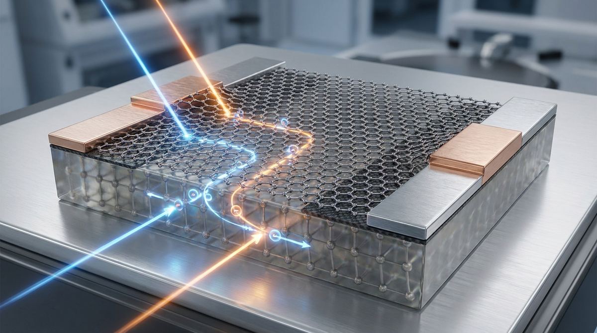
The key idea proposed by the researchers is to optimize the interface using graphene. Graphene is a single layer of carbon atoms arranged in a hexagonal lattice. It is one of the most conductive materials known to science, allowing electrons to move through it with almost no resistance. By integrating graphene into the silicon carbide structure, the researchers aim to create a "super-highway" for charge carriers. This optimization is intended to ensure that once an X-ray creates a charge, those charges are swept away to the electrodes with maximum speed and minimum loss, even if the material itself has been damaged by radiation.
How the Graphene-Based System Works
To understand why this combination is so effective, one must look at the atomic-scale interaction between the graphene layer and the silicon carbide substrate. Silicon carbide is a wide-bandgap semiconductor, meaning it requires a significant amount of energy to move an electron from the valence band to the conduction band. This large bandgap is exactly what makes it radiation-hard, as it is less likely for thermal energy to accidentally kick electrons into the conduction band, which would cause noise.
When we introduce graphene, we are essentially managing the electrical contact between the semiconductor and the external circuitry. In a standard detector, the contact between a metal electrode and a semiconductor can create a Schottky barrier—a physical energy hurdle that electrons must jump over. This barrier increases resistance and slows down the charge extraction process, directly harming the time resolution.
Graphene, however, has an exceptional ability to form high-quality, low-resistance contacts. Because of its unique electronic structure, graphene can be engineered to align its work function with the conduction band of the silicon carbide. This minimizes the height of the energy barrier, allowing charge carriers to flow into the external circuit almost instantaneously. Additionally, the incredibly high carrier mobility of graphene ensures that once the charges leave the silicon carbide, they are transported to the measurement electronics without significant delay.
Furthermore, the presence of graphene can act as a passivation layer. Surface recombination is a major cause of reduced charge collection efficiency, where electrons and holes meet at the surface of the detector and annihilate each other before being measured. The graphene layer covers the surface of the silicon carbide, effectively "plugging" the surface defects and preventing these carriers from being lost at the boundary. This structural synergy—the ruggedness of the silicon carbide combined with the high-speed transport of the graphene—creates a system that is both fast and resilient.
What the Researchers Found
The study conducted by Jiang, Wang, and the team focused on measuring how this graphene-optimized architecture holds up under the stress of X-ray irradiation. The researchers specifically looked at two critical metrics: charge collection efficiency and time resolution.
The results indicated a remarkable degree of stability. In many traditional detectors, intense X-ray exposure leads to a noticeable drop in the amount of charge collected over time. However, the graphene-optimized silicon carbide detector showed that the charge collection efficiency remained highly consistent even as the dose of radiation increased. This suggests that the graphene layer effectively mitigates the impact of radiation-induced traps by facilitating faster charge extraction, essentially "outrunning" the traps.
Even more impressive was the stability of the time resolution. The researchers found that the timing precision of the detector did not degrade significantly under irradiation. This means the detector could maintain its ability to timestamp X-ray events with extreme accuracy, despite being bombarded by high-energy photons. The ability to maintain both high efficiency and high timing precision simultaneously is the "holy grail" of radiation detector design, and the research indicates that the graphene-silicon carbide interface is a viable path toward achieving it.
Why the Result Matters
The implications of these findings are profound for both industrial engineering and fundamental science. In the medical field, specifically in Positron Emission Tomography (PET) and Computed Tomography (CT) scans, the ability to resolve time is everything. Faster time resolution allows for much clearer images with lower radiation doses for the patient. If a detector can maintain its performance over years of heavy use, hospitals can rely on more consistent diagnostic results, leading to better patient outcomes.
In the realm of space exploration, detectors are often the most vulnerable components. Space is filled with high-energy cosmic rays and solar radiation that can slowly "blind" a spacecraft's sensors. A detector that is naturally resistant to radiation-induced degradation could extend the lifespan of deep-space missions, allowing probes to travel further and operate longer in harsh environments like the moons of Jupiter or Saturn.
For particle physics, where detectors are placed near high-intensity beams in accelerators like the Large Hadron Collider, the ability to operate at high rates without performance decay is essential. As physics experiments push for higher luminosities and faster event rates, the demand for detectors that do not "tire" under radiation becomes critical. This research provides a blueprint for the next generation of instrumentation required to unlock the secrets of the subatomic universe.
Limitations and What Still Needs Testing
While the results are highly promising, it is important to distinguish these laboratory successes from commercial readiness. The study demonstrates a significant advancement, but several engineering hurdles remain. First, the process of integrating high-quality, uniform graphene layers onto a silicon carbide substrate is a complex and delicate manufacturing task. Scaling this up from a laboratory-scale prototype to mass-produced, large-area detector arrays will require significant advancements in semiconductor fabrication technology.
Second, while the detector was tested under X-ray irradiation, different types of radiation—such as heavy ions or neutrons—may affect the material in different ways. Future research must investigate how this graphene-optimized system performs against a wider spectrum of particle radiation to ensure complete reliability in diverse environments.
Finally, there is the question of long-term aging. While the detector showed stability under intense, short-term irradiation, the long-term effects of continuous, low-level radiation over many years still require extensive testing. Understanding the cumulative effect of radiation on the graphene-silicon carbide interface will be vital before these detectors can be deployed in mission-critical applications.
Real-World Applications
The potential applications for graphene-optimized silicon carbide detectors span multiple high-tech industries. In medical imaging, these sensors could enable the creation of ultra-fast PET scanners that provide real-time, high-resolution views of metabolic processes, significantly improving the detection of small tumors.
In the aerospace and satellite industry, these detectors could serve as highly reliable radiation monitors and imaging sensors for satellites orbiting in high-radiation belts. Their ability to withstand the harsh environment of space without losing calibration would be a massive advantage for long-duration missions.
In security and industrial inspection, high-speed X-ray sensors are used to scan cargo and sensitive machinery for defects. A more stable and efficient detector would allow for faster scanning throughts, increasing the throughput of security checkpoints without sacrificing the accuracy of the inspection. Finally, in high-energy physics, these detectors will be essential for the next generation of colliders, helping scientists capture incredibly fast events in the subatomic world.
If You Remember One Thing
If you take away only one fact from this research, let it be this: graphene is not just a "miracle material" for electronics; it is a transformative tool for radiation-hardened sensing. By combining graphene's incredible speed with silicon carbide's ruggedness, we are entering an era where detectors can remain ultra-fast and highly accurate even when subjected to the most punishing radiation environments.
FAQ
What exactly is silicon carbide and why is it used in detectors?
Silicon carbide is a semiconductor material characterized by its wide bandgap. This wide bandgap makes it much more resistant to heat and radiation than standard silicon. Because it requires more energy to create unwanted electrical noise, it is ideal for environments where high-energy particles are constantly hitting the sensor.
Why is graphene added to the silicon carbide?
Graphene is added primarily to improve the contact between the semiconductor and the electrical circuit. Because graphene is extremely conductive and has a unique electronic structure, it helps extract charge carriers much faster than traditional metal contacts. This speed is what allows the detector to achieve ultra-fast time resolution.
What is charge collection efficiency and why does it matter?
Charge collection efficiency is a measure of how many of the electrons and holes created by an X-ray actually reach the sensor's electrodes to be measured. If this efficiency is low, the detector produces a weak signal that is hard to distinguish from background noise. High efficiency is crucial for clear, accurate imaging.
How does radiation damage affect a detector's timing?
Radiation creates defects in the crystal structure of the semiconductor, which act like traps for moving charges. When charges get stuck in these traps, it creates a delay and adds electrical noise, making it difficult to precisely timestamp when an event occurred. This loss of timing precision is known as jitter.
Is this technology ready for use in hospitals today?
Not quite yet. While the research shows incredible potential, the technology is currently in the advanced research and development phase. Moving from a laboratory prototype to a standardized, mass-produced medical device requires further testing for long-term stability and more efficient manufacturing processes.
Conclusion
The research conducted by Zhenyu Jiang, Congcong Wang, Jingcong He, Yi Zhan, Yingjie Huang, Xiyuan Zhang, and Xin Shi represents a significant leap forward in detector technology. By leveraging the unique properties of graphene to optimize silicon carbide, they have addressed one of the most persistent problems in radiation sensing: the degradation of performance under stress. As we continue to push the boundaries of what is possible in medical imaging, space exploration, and particle physics, the synergy between graphene and wide-bandgap semiconductors will likely play a central role in the next generation of scientific discovery.