Introduction
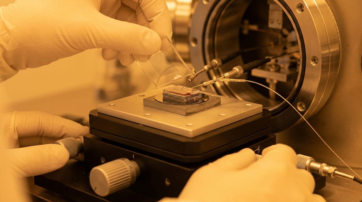
The next generation of low-power electronics requires a shift away from traditional charge-based logic toward devices that leverage the coupling between electric and magnetic orders. This guide outlines the practical implementation of a magnetoelectric switch using a van der Waals (vdW) heterostructure. By combining graphene with the multiferroic material CuCrP2S6, we can create a device where the electrical resistance of the graphene channel is controlled by the electric polarization of the multiferroic layer.
This capability is particularly valuable for non-volatile memory and neuromorphic computing, where the state of the device must be switchable via an electric field but readable via magnetic or electrical means. The core mechanism relies on the interfacial magnetoelectric effect, where the polarization state of the CuCrP2S6 layer modulates the charge-neutrality point in the graphene.
The Engineering Objective
The goal is to fabricate a single-layer graphene channel encapsulated or topped by a layer of CuCrP2S6. The successful prototype must demonstrate three specific behaviors:
1. Hysteresis in the resistance-voltage curve, indicating that the polarization of the CuCrP2S6 has been switched.
2. A shift in the graphene charge-neutrality resistance peak when an in-plane magnetic field is applied.
3. Reversible switching of the transport state through controlled cooling under an applied electric field.
Required Materials and Equipment
To build this prototype, a standard micro-fabrication facility or a high-end specialized nano-lab is required.
1. Graphene: High-quality monolayer graphene, preferably via mechanical exfoliation for research-grade prototypes or CVD for scalable testing.
2. CuCrP2S6: A high-purity flake of the multiferroic material CuCrP2S6, obtained via mechanical exfoliation from a bulk crystal.
3. Substrate: Heavily doped Silicon with a 285 nm SiO2 layer (standard for back-gating) or a specialized gate-dielectric substrate.
4. Transfer Medium: Polycarbonate (PC) or Polydimethylsiloxane (PDMS) on a silicon wafer for the dry-transfer/pick-up method.
5. Lithography: Electron-beam lithography (EBL) system for precise contact patterning.
6. Metallization: Electron-beam evaporator for depositing Titanium/Gold (Ti/Au) contacts.
7. Measurement: A high-precision semiconductor parameter analyzer (e.g., Keithley 4200-UWB) and a cryostat equipped with an in-plane magnetic field capability.
Prototype Fabrication Steps
The fabrication of vdW heterostructures is highly sensitive to interfacial contamination. The pick-up method is the recommended approach to ensure a clean, atomically sharp interface between the graphene and the multiferroic.
1. Substrate Preparation: Clean the SiO2/Si substrate using standard RCA cleaning or oxygen plasma treatment to remove organic residues.
2. Graphene Exfoliation and Pick-up:
- Use a PC-coated silicon wafer to pick up a monolayer of graphene from a graphite substrate via mechanical exfoliation.
- Once the graphene is on the PC film, move the stage to a location where a CuCrP2S6 flake has been exfoliated onto a SiO2 substrate.
- Bring the graphene/PC film into contact with the CuCrP2S6 flake.
- Apply gentle heat (approximately 50 to 110 degrees Celsius, depending on the polymer) to facilitate adhesion and promote the removal of trapped air/bubbles at the interface.
3. Transfer to Target Substrate:
- Once the graphene and CuCrP2S6 are adhered to each other, transfer the stack onto the target SiO2/Si substrate.
- Use a controlled heating and cooling cycle to ensure the stack adheres firmly to the substrate.
4. Contact Patterning:
- Use Electron-beam lithography to define the source and drain electrodes on the graphene layer.
- Perform metal deposition (Ti/Au) via electron-beam evaporation.
- Conduct a post-deposition anneal in a vacuum or forming gas (H2/Ar) to reduce contact resistance.
5. Encapsulation (Optional but Recommended):
- To prevent oxidation of the CuCrP2S6, encapsulate the device with a thin layer of hexagonal Boron Nitride (hBN) using the same pick-up method.
Testing and Characterization Protocol
The testing phase must be conducted in a controlled environment, specifically a cryostat, as the multiferroic properties of CuCrP2S6 are highly temperature-dependent.
1. Charge-Neutrality Point (CNP) Mapping:
- Perform a gate voltage sweep (V_g) while measuring the resistance (R) of the graphene.
- Identify the resistance peak, which represents the charge-neutrality point.
2. Polarization Switching (Hysteresis Test):
- Apply a large DC voltage to the gate/multiferroic layer.
- Sweep the voltage back and forth to observe the hysteresis in the resistance peak. This hysteresis confirms that the electric field has successfully flipped the polarization of the CuCrP2S6.
3. Magnetoelectric Response Test:
- While holding the device at a constant gate voltage, apply an in-plane magnetic field (B-field).
- Monitor the shift in the resistance peak. The shift in the position of the CNP as a function of the magnetic field is the direct signature of the magnetoelectric effect.
4. Domain Control Test:
- Cool the device from room temperature to cryogenic temperatures while applying a constant electric field.
- Observe if the polarization state (and thus the resistance) can be stabilized or reversed by the cooling process.
Engineering Assumptions and Missing Data
Because the source material is a fundamental research paper, several parameters must be assumed for practical engineering implementation:
1. Temperature: The source does not specify the exact temperature required for the multiferroic phase. We assume a starting temperature of 50 Kelvin, cooling down to 10 Kelvin, as most multiferroic orders in these materials are most stable at cryogenic temperatures.
2. Electric Field Strength: The source does not provide the exact voltage required for polarization switching. We assume a gate voltage sweep range of -10V to +10V for initial prototyping.
3. Magnetic Field Strength: The source does not specify the required B-field. We assume an in-plane magnetic field of 1 to 2 Tesla is required to observe a measurable shift in the CNP.
4. Layer Thickness: We assume the CuCrP2S6 layer must be thin enough (a few nanometers) to allow the electric field to penetrate the interface effectively, but thick enough to maintain ferroelectric order.
Technical Risks and Mitigation
1. Interfacial Contamination: The presence of polymer residue or air bubbles between the graphene and CuCrP2S6 will kill the magnetoelectric effect.
- Mitigation: Use the dry-transfer pick-up method and perform high-temperature annealing in a controlled atmosphere.
2. Material Degradation: CuCrP2S6 may be sensitive to ambient moisture and oxygen.
- Mitigation: Always encapsulate the device with hBN or a high-quality dielectric immediately after fabrication.
3. Contact Resistance: High resistance at the Ti/Au/Graphene interface can mask the magnetoelectric signal.
- Mitigation: Use EBL for precise contact placement and perform vacuum annealing to ensure ohmic contacts.
4. Thermal Stress: Rapid cooling in a cryostat can cause the vdW layers to delaminate due to mismatched thermal expansion coefficients.
- Mitigation: Implement a slow, controlled cooling ramp (e.g., 1-2 Kelvin per minute).
Source Basis
This guide is based on the research findings presented in:
Tanaka, M., et al. (2026). Switchable Magnetoelectric Transport in Graphene via a Van der Waals Multiferroic. arXiv:2608.30170v1.