Imagine a material so incredibly thin that it is only one atom thick, yet it possesses the potential to redefine how every electronic device in your pocket functions. This is the promise of graphene, a superstar in the world of materials science. However, graphene is rarely used in isolation; it is almost always placed on a substrate, a supporting material that often dictates how the graphene behaves. The research presented by Ylea Vlamidis, Stiven Forti, Antonio Rossi, Arrigo Calzolari, Carmela Marinelli, Camilla Coletti, Stefan Heun, and Stefano Veronesi offers a groundbreaking way to control this relationship. By strategically inserting a layer of nickel between the graphene and its substrate, these scientists have unlocked a new method to engineer the interface of these materials, creating what is known as a two-dimensional heterostructure. This breakthrough represents a shift from merely observing graphene to actively designing its electronic personality.
The Problem This Research Is Solving
In the quest to develop faster and smaller electronics, scientists face a significant hurdle when working with graphene grown on silicon carbide. While epitaxial graphene on SiC(0001) is an excellent candidate for high-speed transistors, it suffers from a lack of control. When graphene is grown on a silicon carbide substrate through thermal decomposition, a layer of carbon atoms known as the buffer layer is formed. This buffer layer is covalently bonded to the silicon atoms in the substrate, which creates an uncontrolled electrical interaction.
This interaction leads to unintentional doping, where the substrate essentially forces a specific electrical charge into the graphene. For engineers, this is a nightmare. If you want to build a transistor, you need to be able to turn the flow of electricity on and off precisely. If the substrate is already "pre-loading" the graphene with charge, the device becomes difficult to control, making it nearly impossible to create the high-precision components required for modern computing or quantum information processing. The fundamental problem is that the interface between the graphene and the substrate is too rigid and too unpredictable to be used in sophisticated electronic architectures.
The Key Idea in Plain English
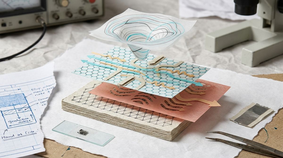
The researchers proposed a solution that sounds like a magic trick: intercalation. To understand this, imagine a sandwich where the bread is graphene and the bottom slice of bread is the silicon carbide substrate. Usually, these two pieces are pressed tightly together, influencing each other. Intercalation is the process of sliding a very thin, single-atom layer of a different material—in this case, nickel—between the two slices.
By sliding nickel atoms into that tiny gap, the scientists can break the rigid chemical bonds that previously tied the graphene to the substrate. This effectively lifts the graphene away from the silicon atoms, creating a new interface. Instead of the graphene being stuck to a semiconductor, it is now sitting on a thin sheet of metal. This transition changes the way electrons move through the graphene, allowing scientists to tune the material's properties with much higher precision than ever before. It essentially transforms a fixed material into a programmable one.
How the Graphene-Based System Works
To understand the mechanics of this system, we must look at the atomic dance occurring at the interface. The starting point is epitaxial graphene grown on the silicon-terminated face of silicon carbide, known as SiC(0001). As the substrate is heated, silicon atoms sublimate, leaving behind a layer of carbon. This carbon layer eventually forms the honeycomb lattice of graphene, but initially, it is chemically tethered to the silicon.
When nickel is introduced into the system—typically through a process of evaporation or deposition followed by controlled heating—the nickel atoms begin to diffuse. Because of the thermal energy provided, the nickel atoms migrate through the gaps in the carbon lattice. This process is driven by thermodynamics; the system seeks a lower energy state, which occurs when the nickel atoms occupy the space between the graphene and the SiC.
As the nickel atoms settle into this interface, they perform a vital task: they disrupt the covalent Si-C bonds. This disruption causes the graphene layer to decouple from the substrate. Once this decoupling occurs, the electronic structure of the graphene is fundamentally transformed. The nickel layer acts as a charge reservoir. Because nickel is a metal, it can donate or accept electrons, a process known as charge transfer. This transfer shifts the Fermi level of the graphene, which is the energy level at which the most important electronic transitions occur. By controlling the amount of nickel present, the researchers can effectively "dial in" the desired electrical state of the graphene, making it a highly versatile platform for creating complex heterostructures.
What the Researchers Found
The core finding of this research is the successful creation of a novel platform for engineering two-dimensional heterostructures. The team demonstrated that nickel intercalation is a viable and effective method for modifying the interface of epitaxial graphene on SiC. Rather than just seeing a random change in conductivity, the researchers found that they could create a structured, predictable environment.
The study suggests that by using nickel, they have created a way to decouple the graphene from the substrate's influence while simultaneously introducing a new, controllable electronic influence. This results in a system where the properties of the graphene are no longer dictated by the substrate, but are instead dictated by the specific characteristics of the nickel layer. This level of control is the holy grail of 2D materials science, as it allows for the creation of interfaces that do not exist in nature, providing a clean slate for testing new theories in condensed matter physics and material science.
Why the Result Matters
The significance of this work cannot be overstated for the future of nano-electronics. In traditional silicon-based technology, we are reaching the physical limits of how small and efficient we can make transistors. Graphene offers a path forward, but only if we can control it. This research provides a toolset to move from the "discovery" phase of graphene research into the "engineering" phase.
When we can control the electronic properties of a material at the atomic scale, we can create devices that are faster, smaller, and consume significantly less power. Furthermore, this research provides a playground for quantum computing. Quantum bits, or qubits, require extremely stable and highly controlled environments to function without error. A tunable, two-dimensional heterostructure created through intercalation could provide the precise electronic environments needed to host and manipulate quantum states. The ability to engineer the interface means we can potentially design the exact conditions required for specific quantum phenomena to emerge.
Limitations and What Still Needs Testing
While this research is a significant leap forward, it is important to recognize that it is not yet ready for mass production. The process of intercalation is highly sensitive to temperature, time, and the purity of the materials used. Achieving a perfectly uniform layer of nickel atoms across a large-scale wafer is an enormous engineering challenge. If the nickel layer is uneven, the graphene will have inconsistent electrical properties across its surface, which would render it useless for high-precision electronics.
Additionally, the long-term stability of these heterostructures under operational conditions must be tested. In a real-world device, the material will be subjected to heat, electrical currents, and environmental moisture. Scientists must determine if the nickel atoms stay in their intercalated position or if they migrate over time, which would change the device's performance. Finally, the scalability of this process—moving from a small laboratory sample to a large-scale industrial manufacturing process—remains a significant hurdle that must be addressed before this technology can appear in consumer electronics.
Real-World Applications
The potential applications for nickel-intercalated graphene span several high-tech industries. In the realm of high-frequency electronics, these materials could be used to create transistors that operate at much higher speeds than current silicon technology, enabling faster telecommunications and more responsive processing units.
In the field of sensing, the high surface-to-volume ratio of graphene combined with the tunable electronic properties provided by nickel intercalation could lead to ultra-sensitive chemical and biological sensors. Such sensors could detect single molecules, opening new doors in medical diagnostics and environmental monitoring. Furthermore, as mentioned previously, the field of quantum technologies stands to benefit immensely, with these heterostructures serving as a foundation for more stable and scalable quantum architectures.
If You Remember One Thing
If there is one takeaway from this research, it is that the interface is just as important as the material itself. By mastering the art of intercalation, scientists are no longer limited by the properties of the materials they start with; they are gaining the ability to design entirely new electronic environments at the atomic level.
FAQ
What exactly is intercalation in the context of this research?
Intercalation is a process where small atoms or molecules are inserted into the spaces between the layers of a material. In this study, nickel atoms were inserted between the graphene layer and the silicon carbide substrate to change how the graphene behaves electronically.
Why is silicon carbide used as a substrate for graphene?
Silicon carbide is a common substrate for growing epitaxial graphene because it is a semiconductor that can be thermally decomposed to leave behind high-quality, single-crystal graphene layers. It provides a stable, crystalline foundation for the carbon atoms.
What is a two-dimensional heterostructure?
A heterostructure is a structure made of different types of materials layered together. A two-dimensional heterostructure is a special type where the layers are incredibly thin, often just one or two atoms thick, allowing for extremely precise control over how electrons move across the interface.
How does nickel change the properties of graphene?
Nickel changes graphene by breaking the chemical bonds between the graphene and the silicon carbide substrate. Once those bonds are broken, the nickel atoms act as a source of charge, which can be used to tune the electrical conductivity and the energy levels of the graphene.
Is this technology ready to be used in smartphones today?
No, this technology is still in the research and development stage. While it shows immense promise, scientists still need to figure out how to make this process uniform over large areas and ensure that the materials remain stable over long periods of time in real-world conditions.
Conclusion
The work by Vlamidis, Forti, Rossi, Calzolari, Marinelli, Coletti, Heun, and Veronesi marks a vital step in the evolution of two-dimensional materials. By utilizing nickel intercalation to engineer the interface between graphene and silicon carbide, they have provided a new platform for creating highly tunable and programmable heterostructures. While significant engineering challenges remain regarding scalability and stability, the ability to precisely control electronic properties at the atomic scale opens a new frontier for the next generation of electronics, sensors, and quantum computers.