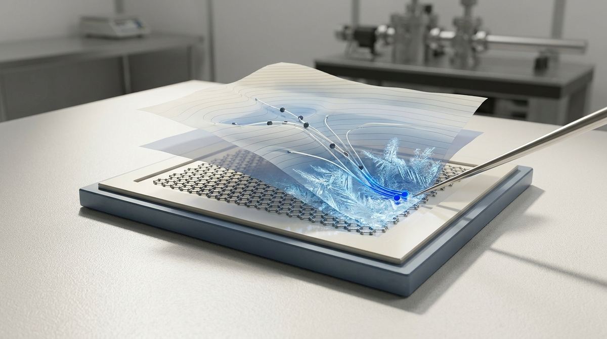
Inside every graphite pencil is a structure of carbon that is almost perfect, but not quite perfect enough for the next generation of quantum technology. For years, scientists have struggled to peel these layers apart without damaging them or leaving behind chemical residue that slows down the very electrons they are trying to guide. The secret to unlocking the next generation of super-fast electronics might lie in how we shake up the very structure of graphite using extreme cold. By using sudden, intense temperature shifts, scientists can now manipulate the fundamental arrangement of carbon atoms, opening a door to a rare form of graphite that moves electricity with unprecedented speed.
The Problem This Research Is Solving
The fundamental challenge in carbon-based electronics is the specific way the carbon atoms are stacked within a crystal. Most graphite encountered in nature and industry follows a Bernal stacking pattern, commonly known as AB stacking. In this arrangement, the layers are offset in a specific way that makes them incredibly stable but electronically limited. While Bernal graphite is an excellent conductor, it lacks the exotic electronic properties required for advanced applications like topological quantum computing or ultra-low-power transistors. To achieve these goals, scientists need rhombohedral graphite, also known as ABC stacking.
Rhombohedral graphite is fundamentally different because its atomic arrangement creates flat bands in its electronic structure. In standard materials, electrons move through a landscape of varying energy levels. In rhombohedral graphite, these flat bands create a high density of states, which allows for much more interesting electron-electron interactions. However, rhombohedral graphite is much harder to isolate in a clean, high-quality state. Usually, when you try to separate graphite layers to study them, you face a trade-off. Chemical exfoliation, which uses acids or solvents to push layers apart, often leaves behind tiny impurities or defects. These defects act as roadblocks, or scattering centers, for moving electrons. When an electron hits a defect, it loses energy and momentum, which drastically reduces the mobility of the material. For nanoelectronics, where every single atom counts, this loss of performance is a deal-breaker.
The Key Idea in Plain English
The researchers have proposed a solution that uses physics rather than chemistry: cryogenic shock exfoliation. Instead of using a liquid to dissolve the bonds between layers, this method uses the physical stress caused by extreme temperature changes. When a material is suddenly moved from room temperature to a state of extreme cold, the atoms within the lattice contract. Because different parts of the crystal or the substrate it sits on might contract at different rates, a mechanical stress is generated between the layers.
This stress acts like a microscopic wedge. It provides just enough force to overcome the weak van der Waals forces that hold the carbon layers together, popping them apart without the need for harsh chemicals. Because no chemicals are used, the resulting flakes are incredibly clean. This cleanliness is the key to achieving ultrahigh mobility, as it ensures that the path for the electrons remains unobstructed by foreign atoms or structural damage.
How the Graphene-Based System Works
To understand why this works, we have to look at the relationship between atomic structure and electron movement. In a solid material, the mobility of a charge carrier—such as an electron—is determined by how much it is scattered as it travels through the crystal lattice. This scattering is caused by several factors: lattice vibrations (phonons), impurities, and structural defects like missing atoms or misplaced layers. If the mobility is high, the electron can travel a long distance before its momentum is interrupted.
In the rhombohedral system developed by Ludwig Holleis, Youngjoon Choi, Canxun Zhang, Jack H. Farrell, Gabriel Bargas, Audrey Hsu, Zexing Chen, Ian Sackin, Wenjie Zhou, Yi Guo, Thibault Charpentier, Yifan Jiang, et al., the focus is on minimizing these scattering events. When the cryogenic shock is applied, the thermal contraction creates a precise mechanical strain. This strain is directed along the interlayer axis, meaning the force is applied exactly where the layers are most weakly bonded.
By controlling the rate and intensity of the temperature shift, the researchers can manage the amount of energy released into the crystal. This energy is sufficient to break the van der Waals bonds but is not high enough to break the much stronger covalent bonds within the carbon sheets themselves. This distinction is vital. If the energy were too high, the carbon layers themselves would shatter or become distorted, creating the very defects the researchers are trying to avoid. By keeping the shock controlled, the rhombohedral stacking order (ABC) is preserved, and the resulting flakes possess a highly ordered atomic landscape. This order allows the electrons to behave according to the unique physics of the rhombohedral band structure, moving through the lattice with almost no resistance.
What the Researchers Found
The primary finding of this research is the successful creation of rhombohedral graphite flakes with ultrahigh mobility. This means the researchers were able to demonstrate that the cryogenic shock method produces a material where electrons can move with much higher velocity and for longer distances compared to traditionally exfoliated or chemically treated graphite.
The research confirms that rhombohedral stacking can be maintained even after the mechanical stress of exfoliation. This is a significant technical achievement because the ABC stacking sequence is often less thermodynamically stable than the AB sequence in many environments. The ability to isolate these flakes while preserving their unique electronic properties proves that thermal-mechanical manipulation is a viable pathway for studying and utilizing exotic carbon phases. The data suggests that the reduction in impurity-driven scattering is the direct cause of the observed increase in carrier mobility, validating the idea that "clean" exfoliation is superior to "chemical" exfoliation for high-end electronic applications.
Why the Result Matters
This result is significant because it bridges the gap between theoretical physics and practical materials engineering. For decades, the concept of using rhombohedral graphite for electronics was largely a theoretical pursuit because no one could produce a sample clean enough to measure its true potential. By proving that ultrahigh mobility can be achieved, this research moves the field closer to actual device fabrication.
From an engineering perspective, high mobility translates directly to speed and efficiency. In a transistor, the speed at which a device can switch from an "on" to an "off" state is limited by how fast the charge carriers can move through the channel. If we can use rhombohedral graphite to create transistors that operate at much higher frequencies with less heat generation, we could see a revolution in computing power. Furthermore, the unique topological properties of rhombohedral graphite could lead to the development of "topological electronics," where electron flow is protected by the material's own symmetry, making it nearly immune to the noise and interference that plague current silicon-based chips.
Limitations and What Still Needs Testing
While this is a major breakthrough, it is important to distinguish these laboratory successes from commercial readiness. Currently, the cryogenic shock method is a precise, controlled process used to create small, high-quality flakes for scientific study. It is not yet a scalable manufacturing process. Scaling this up to create large-area films of rhombohedral graphite for use in mass-produced microchips remains a massive engineering hurdle.
Additionally, the stability of these rhombohedral structures must be tested over longer periods and under different environmental conditions. While the material may be stable at the cryogenic temperatures used in the lab, its behavior at room temperature and its long-term durability in various electronic packaging environments need further investigation. There is also the question of how this material will interface with other common semiconductor materials, as the interface between two different materials often introduces new defects that could negate the benefits of the high-mobility graphite.
Real-World Applications
The potential applications for ultrahigh-mobility rhombohedral graphite are vast, particularly in the high-tech sector. One of the most promising areas is quantum computing. The unique electronic states found in ABC-stacked graphite could be used to create topological qubits. These qubits would be significantly more stable and less prone to "decoherence," which is the primary obstacle to building large-scale, error-free quantum computers.
Another application is in the field of ultra-high-speed sensors. Because the electronic properties of these materials are so sensitive to external stimuli due to their unique band structures, they could be used to create sensors that can detect incredibly minute changes in electric fields, pressure, or chemical concentrations. Finally, in the realm of classical nanoelectronics, rhombohedral graphite could pave the way for a new class of low-power processors that operate with much higher efficiency than current silicon-based technology, potentially reducing the energy consumption of massive data centers.
If You Remember One Thing
If you remember only one thing from this research, let it be this: the way we manipulate materials at the atomic level—using tools like cryogenic shock—is unlocking entirely new phases of matter that could lead to the next era of lightning-fast, ultra-efficient electronics.
FAQ
Question: What is the difference between Bernal and Rhombohedral graphite?
Answer: Bernal graphite, or AB stacking, is the standard, stable form of graphite where layers are offset in a way that is common in nature. Rhombohedral graphite, or ABC stacking, is a different arrangement of those same carbon layers that results in much more complex and interesting electronic behaviors, such as flat energy bands.
Question: Why is cryogenic shock better than chemical exfoliation?
Answer: Chemical exfoliation uses liquids and acids to separate layers, which often leaves behind chemical residue or impurities. These impurities act as obstacles that slow down electrons. Cryogenic shock uses rapid temperature changes to create mechanical stress that separates the layers cleanly, without leaving any residue behind, leading to much higher electron mobility.
Question: What does ultrahigh mobility actually mean for a computer chip?
Answer: Mobility refers to how easily and quickly an electron can move through a material. In a computer chip, higher mobility means that the electrons can move through the transistors faster, allowing the chip to operate at higher speeds and with less energy loss, which reduces heat and increases performance.
Question: Why can't we use this in our phones right now?
Answer: This research is currently in the fundamental science stage. While the researchers have successfully created high-quality samples in a laboratory setting, scaling this process up to produce large, continuous sheets of material for mass manufacturing is a much more complex engineering challenge that has not yet been solved.
Question: Is rhombohedral graphite a new material or just a different form?
Answer: It is a different structural form, or polymorph, of the same element: carbon. Just as diamond and graphite are both forms of carbon with different structures and properties, rhombohedral graphite is a specific structural arrangement that offers different electronic advantages compared to the common form of graphite.
Conclusion
This research points toward a practical lesson: graphene-based materials are most powerful when their nanoscale properties are connected to a clear engineering problem. The result is not a finished commercial product by itself, but it gives researchers and manufacturers a better map for designing lighter, more sensitive, or more durable systems. Future work still needs testing under real operating conditions, but the direction is promising because it joins materials science with application-driven design.