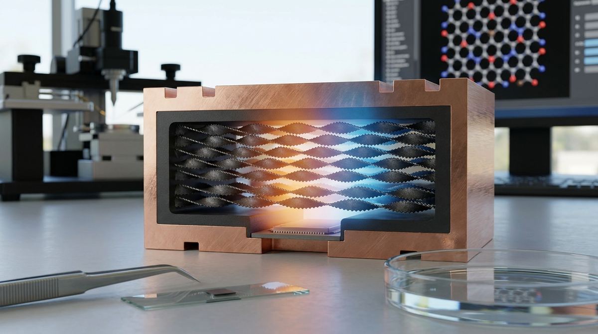
Imagine if we could build the fundamental components of a supercomputer not by carving silicon, but by arranging individual atoms like tiny pieces of origami. This is the frontier of nanotechnology, where the shape of a single edge can determine whether a material acts as a conductor or an insulator. Recent breakthroughs in the synthesis of graphene nanoribbons are bringing us closer to this reality. By moving beyond simple sheets of carbon and into the realm of highly specific, asymmetrical shapes, researchers are unlocking a new way to control how electricity and heat flow through matter. This work, involving the detailed study of how geometry dictates function, represents a critical step toward the next generation of nano-electronics.
The Problem This Research Is Solving
To understand why this research is vital, one must first understand the "graphene paradox." Graphene is a single layer of carbon atoms arranged in a hexagonal lattice, famous for being incredibly thin and exceptionally conductive. In its pristine, perfectly flat, and infinite sheet form, graphene is a zero-bandgap semi-metal. In the world of digital computing, this is a significant obstacle. A computer's brain, the microprocessor, relies on transistors that act as tiny on and off switches. To turn a switch off, a material must have a "bandgap"—a specific energy range where electrons are forbidden from moving. Because pristine graphene has no such gap, it cannot be easily "turned off," making it difficult to use in the logic-based circuits that power everything from smartphones to supercomputers.
Beyond the electronic problem, there is the issue of thermal management. As electronic devices get smaller and more powerful, they generate concentrated heat. If we cannot control how heat moves through a material at the nanoscale, the device will melt or fail. In traditional materials, heat is carried by lattice vibrations, also known as phonons. In graphene, these phonons travel incredibly fast, but managing that heat in a microscopic circuit requires a deep understanding of how the edges of a material interfere with these vibrations. Current manufacturing methods often produce irregular, messy edges that scatter electrons and heat unpredictably, leading to inefficient and unreliable devices.
The Key Idea in Plain English
The solution proposed by the scientific community involves transforming graphene from a simple sheet into "nanoribbons." By cutting graphene into extremely narrow strips, we can force the electrons into a confined space. This confinement naturally creates the bandgap that pristine graphene lacks, finally giving us the "off switch" needed for digital logic. However, simply making a narrow ribbon is not enough; the shape of the edges matters immensely.
This research focuses on two specific geometric features: gulf-edged structures and chirality. A "gulf-edged" ribbon is one where the edges are not straight lines but instead follow a rhythmic, undulating pattern, similar to a coastline with small bays or gulfs. "Chirality" refers to a property of asymmetry, much like a human hand; a chiral ribbon has a "handedness" that prevents it from being superimposed on its mirror image. When you combine a specific edge shape with a specific twist or handedness, you create a highly specialized environment for electrons and heat. This allows engineers to "tune" the material, selecting the exact electronic and vibrational properties required for a specific task.
How the Graphene-Based System Works
The creation of these sophisticated structures requires a method known as on-surface synthesis. Unlike traditional methods that might involve cutting bulk graphite with harsh chemicals, on-surface synthesis is an incredibly precise process performed in a vacuum on a metal substrate. The researchers, including Xuanchen Li, Amogh Kinikar, Vikas Sharma, Andres Ortega Guerrero, George F. S. Whitehead, Mickael Lucien Perrin, Carlo A. Pignedoli, Roman Fasel, Ashok Keerthi, and Gabriela Borin Barin, utilize specific precursor molecules that are deposited onto a surface.
When these molecules are heated, they undergo a series of chemical reactions, stitching themselves together into long, continuous ribbons. Because the molecules are placed on a metal surface that acts as a template, the resulting ribbon follows the exact atomic blueprint of the precursors. This allows for the creation of the "gulf" indentations and the "chiral" twists with atomic precision. The metal substrate plays a dual role: it provides the catalytic energy needed for the molecules to bond and provides a platform for scientists to observe the resulting structure using advanced tools like Scanning Tunneling Microscopy (STM). This level of control ensures that every atom is in its intended place, which is the only way to ensure the electronic and vibrational properties remain predictable.
What the Researchers Found
The study investigated how these complex geometries—the combination of gulf-edged patterns and chirality—alter the fundamental physics of the ribbon. The researchers focused on two main areas: the electronic properties (how electrons move) and the vibrational properties (how phonons move).
The findings revealed that the specific geometry of a gulf edge significantly modifies the electronic density of states. In simpler terms, the indentations at the edge create new energy levels where electrons can reside or move. This is a direct cause-and-effect relationship: the physical shape of the edge dictates the energy landscape available to the electrons. Furthermore, the introduction of chirality breaks the mirror symmetry of the ribbon. This symmetry breaking is profound because it can lead to unique electronic states that are not present in straight, non-chiral ribbons. These states are essential for developing specialized quantum components where the direction of electron flow is critical.
Regarding vibrational properties, the research demonstrated that the periodic indentations of the gulf edges act as scattering centers for phonons. Because heat is carried by these vibrations, the shape of the edge directly influences the thermal conductivity of the nanoribbon. The way these vibrations interact with the electronic states is also crucial; when a phonon scatters off an electron, it can transfer energy, which is a primary mechanism for electrical resistance. By understanding the relationship between the edge shape, the phonon modes, and the electronic states, the researchers have provided a roadmap for designing materials that can simultaneously optimize electrical conductivity and thermal management.
Why the Result Matters
This research is a cornerstone for the future of condensed matter physics and materials science. For the engineering community, the ability to predict and control these properties is the difference between a theoretical curiosity and a functional component. If we can design a nanoribbon with a specific bandgap, we can create transistors that operate at much higher speeds and lower power than silicon-based counterparts.
Furthermore, the implications for quantum information science are significant. Many quantum computing concepts rely on the specific way electrons behave in asymmetric environments. By using chiral, gulf-edged ribbons, scientists may be able to create "topological" protection, where the movement of electrons is shielded from local disturbances, making quantum information much more stable. The categories of this research, such as condensed matter and the Hall effect, suggest that these materials could also play a role in high-precision metrology, where the standard for electrical resistance is defined by quantum phenomena.
Limitations and What Still Needs Testing
While these findings are groundbreaking, it is important to distinguish between laboratory success and commercial readiness. Currently, on-surface synthesis is a highly controlled, vacuum-based process typically performed at extremely low temperatures. This makes the process slow and expensive, meaning these nanoribbons cannot yet be mass-produced on a semiconductor wafer like silicon chips are today.
Additionally, the study focuses heavily on the theoretical and simulated aspects of how these properties behave in an idealized environment. In a real-world electronic device, the presence of unintended defects, impurities, or the interface between the graphene and the device housing could drastically change how the ribbon behaves. Future research must move from the perfect vacuum of a laboratory to the messy, complex environment of actual electronic circuits. We still need to test how these chiral structures maintain their properties when integrated into larger, multi-layered device architectures.
Real-World Applications
The transition from lab to life will likely occur in three distinct stages. First, we expect to see these materials in specialized sensing applications. Because the electronic properties of these nanoribbons are so sensitive to their edges and surroundings, they could be used to create sensors capable of detecting a single molecule or a minute change in temperature with unprecedented accuracy.
Second, as manufacturing techniques improve, they may find their way into ultra-high-speed, low-power processors for specialized high-performance computing, such as in AI processing units or supercomputing clusters where heat dissipation is a constant battle. Finally, the most transformative application lies in quantum computing. The ability to engineer specific, protected electronic states through chirality and edge-shaping could lead to the creation of qubits that are much more resistant to the "noise" that currently plagues quantum systems.
If You Remember One Thing
If there is one takeaway from this research, it is that the shape of a material is just as important as the material itself. In the world of nanotechnology, the "edge" is not just a boundary; it is a programmable feature that can be used to control electricity and heat with atomic precision.
FAQ
What exactly is a graphene nanoribbon?
A graphene nanoribbon is a long, narrow strip of carbon atoms taken from a larger sheet of graphene. While a flat sheet of graphene conducts electricity very easily and cannot be turned off, cutting it into a narrow ribbon changes its fundamental physics, allowing it to act more like a traditional semiconductor.
Why do the edges of the ribbon matter so much?
In a material this small, the edge represents a huge percentage of the total material. The arrangement of atoms at the edge determines how electrons are confined and how heat vibrations are scattered. By changing the shape of the edge, such as making it wavy or "gulf-edged," we can fundamentally change how the material behaves.
What does "chiral" mean in the context of graphene?
Chirality refers to a lack of mirror symmetry. If a nanoribbon is chiral, it means that its structure looks different if you try to reflect it in a mirror, much like how your left hand is a mirror image of your right hand but they cannot be perfectly aligned. This asymmetry is a powerful tool for controlling the direction and behavior of electrons.
What is on-surface synthesis?
On-surface synthesis is a highly precise manufacturing method where molecules are placed on a flat surface, like a metal, and then heated. The surface acts as a guide, helping the molecules bond together in a very specific, predetermined pattern. This allows scientists to build structures atom-by-atom.
Is this technology going to replace silicon in our phones soon?
It is unlikely in the immediate future. While these nanoribbons offer incredible potential, the current manufacturing process is far too specialized and expensive for mass production. We first need to find ways to create these structures at scale and integrate them into existing electronics manufacturing workflows.
Conclusion
The study of gulf-edged chiral graphene nanoribbons represents a masterclass in atomic-scale engineering. By moving beyond the simplicity of flat sheets and embracing the complexity of asymmetrical, patterned edges, researchers are gaining the ability to dictate the electronic and thermal properties of matter. While challenges in scalability and environmental stability remain, the fundamental understanding gained here provides the blueprint for a future where electronics are defined by their geometry, leading to faster, smaller, and more efficient quantum technologies.