The Physics of Controlled Folding
In the field of 2D materials, we have long treated graphene as a nearly perfect, flat sheet. However, the real power of graphene for industrial applications lies in its ability to transition from a 2D sheet into a 3D architecture. This transition is driven by topological defects known as disclinations. A disclination is essentially a localized error in the hexagonal lattice of graphene that forces the sheet to curve.
Recent research by Yamaletdinov, Katsnelson, and Yazyev has revealed a critical asymmetry in how these defects behave. In a standard model, one might assume that positive disclinations (which create cone-like, convex shapes) and negative disclinations (which create saddle-like, concave shapes) would behave symmetrically. This is not the case.
The research shows that while positive disclinations tend to repel one another, negative disclinations exhibit a robust, long-range attraction. Furthermore, these negative disclinations do not follow the standard saddle-shaped geometry predicted by previous models; instead, they exhibit a sublinear energy scaling that leads to much more complex, irregular morphologies. For an engineer, this is a breakthrough: it means we can use negative disclinations as "attractors" to drive the self-assembly of graphene into complex 3D scaffolds without needing external mechanical force.
The Engineering Objective: 3D Architectures
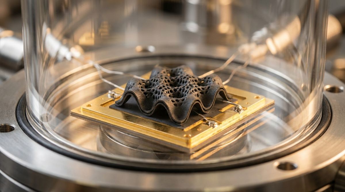
The goal of this guide is to design a method for creating self-folding graphene scaffolds. By strategically patterning negative disclinations into a graphene membrane, we can induce the sheet to fold in on itself, creating a highly porous, 3D interconnected network.
This 3D architecture is specifically intended for high-performance electrochemical applications, such as supercapacitor electrodes or battery current collectors. In a standard flat graphene electrode, the surface area is limited by the geometric footprint of the material. In a self-folded scaffold, the effective electrochemical surface area (ECSA) is dramatically increased due to the complex, saddle-shaped folds and the interconnected pores created by the attraction of negative disclinations.
Required Materials and Equipment
To attempt this prototype, you will need access to a cleanroom environment or a high-end microfabrication lab. The process requires precise control over defect density.
1. Graphene Source: High-quality, large-area monolayer graphene grown via Chemical Vapor Deposition (CVD) on copper foil.
2. Transfer Polymer: Poly-methyl methacrylate (PMMA) for the wet transfer process.
3. Target Substrate: A sacrificial or supporting substrate, such as Silicon/Silicon Dioxide (Si/SiO2) or a flexible polymer like Polyethylene Terephthalate (PET) for flexible electronics applications.
4. Defect Engineering Tool: A Focused Ion Beam (FIB) system or an Electron Beam Lithography (EBL) system coupled with an oxygen plasma etcher.
5. Characterization Tools: An Atomic Force Microscope (AFM) for surface morphology and a Scanning Electron Microscope (SEM) for structural imaging.
6. Electrochemical Testing Setup: A standard three-electrode cell for Cyclic Voltammetry (CV) and Electrochemical Impedance Spectroscopy (EIS).
Prototype Fabrication Process
The following steps outline the process for creating a patterned, self-folding graphene scaffold. Note that the exact parameters for ion dose and etching time are engineering assumptions based on the physics described in the source research.
1. Graphene Growth and Transfer: Grow monolayer graphene on copper using standard CVD methods (typically using methane as a carbon source). Transfer the graphene onto your target substrate (e.g., SiO2/Si) using the PMMA-assisted wet transfer method. Ensure the graphene is clean and free of polymer residue, as impurities will interfere with the disclination-driven folding.
2. Defect Patterning: This is the most critical step. You must create negative disclinations. Using a Focused Ion Beam (FIB), you will bombard specific coordinates on the graphene sheet with ions (such as Argon) to create localized lattice disruptions.
To achieve the "attraction" effect described in the research, you should pattern pairs of negative disclinations at specific intervals. Based on the research's findings on long-range attraction, a starting distance of 500 nanometers to 2 micrometers between defect sites is a cautious starting range for testing.
3. Controlled Release: Once the defects are patterned, the graphene must be released from the substrate to allow it to fold. If you are using a rigid substrate like SiO2, this may require a selective etching process to create "hinges" or to partially lift the graphene. If you are using a flexible substrate, the folding may be triggered by thermal activation or controlled humidity changes.
4. Self-Assembly: As the graphene is released, the negative disclinations will begin to attract one another, driving the sheet to fold into a complex, saddle-shaped 3D morphology.
Testing and Validation Protocol
Once the scaffold is formed, you must validate that the morphology is indeed driven by the disclination attraction and that it provides the intended surface area benefits.
1. Morphological Validation: Use AFM to measure the height and curvature of the folds. You are looking for the deviation from the standard saddle shape mentioned in the research. Use SEM to observe the overall 3D connectivity of the scaffold. A successful prototype will show a high degree of interconnectedness rather than isolated wrinkles.
2. Electrochemical Surface Area (ECSA) Measurement: Perform Cyclic Voltammetry (CV) in a non-faradaic region (where no redox reactions occur) using a standard electrolyte (such as 1M KOH or H2SO4). The double-layer capacitance (Cdl) derived from the CV curve can be used to calculate the ECSA. Compare this value to a flat, non-patterned graphene control sample.
3. Stability Testing: Subject the scaffold to multiple charge-discharge cycles to ensure that the self-folded structure remains stable and does not collapse into a flat sheet under electrochemical stress.
Engineering Assumptions and Limitations
It is vital to distinguish between the scientific findings and the engineering application. The source research proves that negative disclinations attract and exhibit complex energy scaling. However, the following points are engineering assumptions required to make this a practical guide:
- Defect Density: The research does not specify the exact ion dose required to create a single disclination. We assume a dose in the range of 10^12 to 10^14 ions/cm^2 is required to create a localized defect without destroying the entire lattice.
- Patterning Precision: We assume that current FIB or EBL technology is precise enough to place these defects at the nanometer scale required to observe the long-range attraction.
- Substrate Interference: The research focuses on free-standing membranes. In a real-world engineering application, the substrate's adhesion to the graphene may counteract the disclination-driven folding. The "release" step is a significant engineering challenge that requires further optimization.
- Scaling: While the physics works at the microscopic scale, scaling this to a large-scale industrial electrode remains a significant hurdle. The focus should initially be on small-scale, high-value applications like specialized sensors or high-performance micro-supercapacitors.