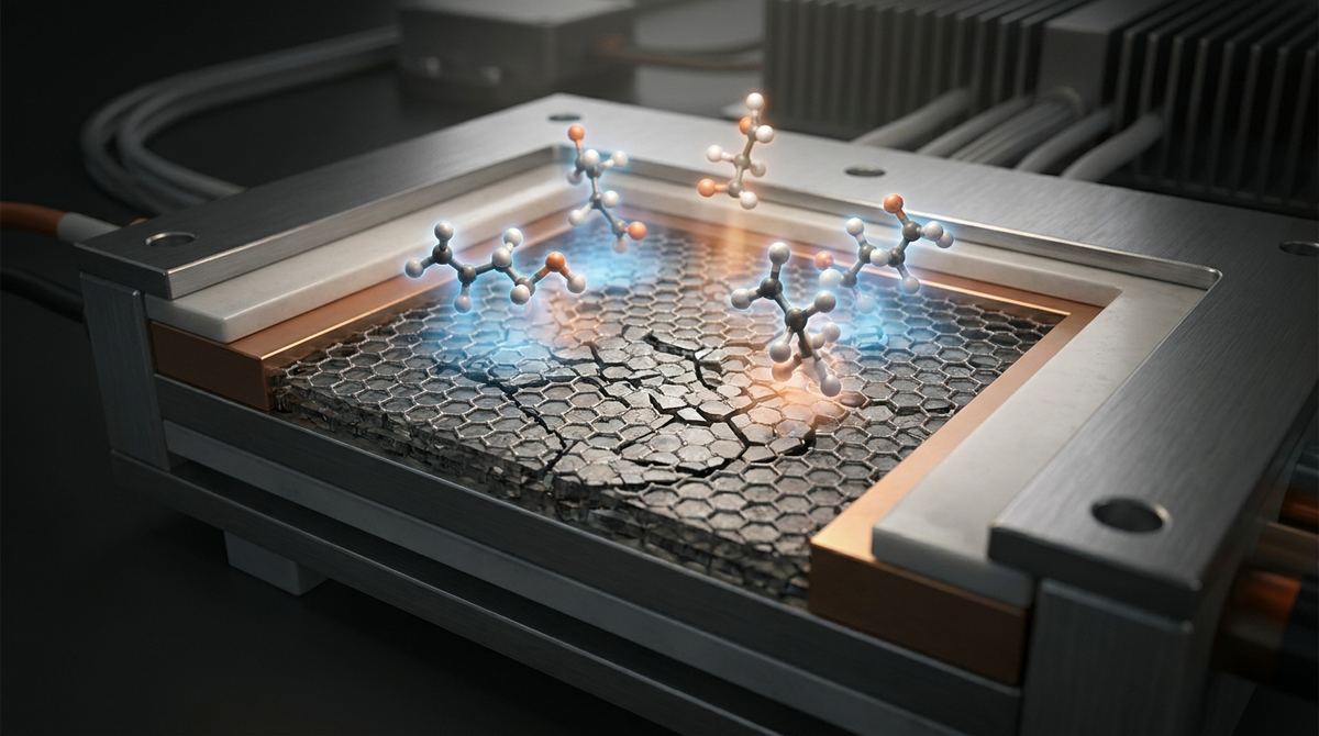
Imagine looking at a perfectly tiled floor where every square is identical and every line is straight. This is how scientists study crystals, the building blocks of most advanced technology. Now, imagine that same floor, but instead, the tiles are shattered, broken into different shapes, and scattered randomly across the room. This is the world of amorphous materials. For decades, engineers and physicists have struggled to predict how these disordered materials will behave because they lack the predictable, repeating patterns found in crystals. If we cannot predict how they conduct electricity or how they bend, we cannot use them to build the next generation of ultra-fast computers or flexible sensors. To solve this, a team of researchers including Le-Ye Zhu, Xi Zhang, Yun-Peng Wang, Jieheng Shi, Junwei Zhang, Shixuan Du, and Yu-Yang Zhang has introduced a way to model this chaos. By rethinking how we view the irregular landscape of a monolayer amorphous material, they have provided a mathematical bridge between the predictable world of order and the unpredictable world of disorder.
The Problem This Research Is Solving
The fundamental challenge in materials science is the ability to predict properties before a material is ever manufactured. When dealing with crystalline materials, such as single-crystal silicon or graphene, the atoms follow a strict, repeating geometric pattern. Because of this periodicity, scientists can use a tiny slice of the material—a single unit cell—to mathematically represent the entire structure. If you know what happens to one atom in the pattern, you know what happens to a billion atoms. This symmetry makes the math relatively simple and the simulations incredibly fast.
However, amorphous materials break these rules. In an amorphous monolayer, the atoms are arranged without long-range order. There is no repeating unit cell, no symmetry, and no predictable pattern. This lack of structure creates a massive computational nightmare. To simulate an amorphous material using traditional methods, scientists must simulate thousands or even millions of individual atoms, each with its own unique surroundings, to capture the true essence of the disorder. This requires massive supercomputing power and an enormous amount of time.
Furthermore, the disorder itself creates physical problems. In crystalline materials, electrons move through the periodic lattice like a wave through a clear medium. In amorphous materials, the irregular arrangement of atoms acts like obstacles, scattering the electrons and significantly changing the material's electrical conductivity. If we cannot model these scattering events accurately because the material is too complex to simulate, we cannot design better semiconductors or more efficient electronics. The scientific community has been stuck between two extremes: the simplicity of crystal models and the overwhelming complexity of full atomistic simulations.
The Key Idea in Plain English
The breakthrough proposed by Zhu, Zhang, Wang, Shi, Zhang, Du, and Zhang lies in a clever way of looking at the chaos. Instead of seeing an amorphous material as a completely random mess, they suggest we should view it as a mosaic of many different tiny, ordered pieces. They call this the polymorphic crystallites model.
To understand this, think of the shattered floor again. While the whole floor looks random, if you look closely at the broken pieces, many of them might still have straight edges or recognizable geometric shapes. These are not the original tiles, but they are structured pieces of them. In the context of atoms, the researchers suggest that even in a disordered sheet, there are small clusters of atoms that form local, semi-ordered patterns. These patterns are not identical—some might look like hexagonal rings, while others might look like pentagons or other shapes.
By treating the amorphous material as a collection of these different, shifting structural motifs—or polymorphic crystallites—the researchers can create a mathematical way to describe the material without having to track every single atom's position. It is a way of saying that while the whole thing is disordered, the disorder is made up of a predictable variety of local orders. This turns a problem of total chaos into a problem of statistical distribution, which is much easier for computers to handle.
How the Graphene-Based System Works
The mechanism of this model relies on identifying the different types of local atomic arrangements that can exist within a thin, two-dimensional sheet. In a monolayer material, which is only one atom thick, the constraints are even higher than in a bulk material. The atoms have fewer neighbors, and the way they bond determines everything about the material's physical properties.
The polymorphic crystallites model works by characterizing these local environments. In a crystalline material, there is only one type of local environment. In an amorphous material, there is a spectrum. The model identifies the most common "polymorphic" versions of local structures that occur when a material is disordered. It then uses a statistical approach to determine how these different motifs are distributed across the material.
This approach essentially acts as a middle ground. On one end, you have the perfect crystal where every site is identical. On the other end, you have a completely random system where every site is unique. The polymorphic crystallites model populates the space between these two extremes. It allows researchers to simulate the material by sampling from a library of these different structural motifs.
When an electron moves through this modeled system, it interacts with these varying motifs. The model can calculate how an electron is scattered when it moves from a hexagonal-like cluster to a pentagon-like cluster. By understanding how these specific local structures affect the movement of charge carriers, the model can predict the overall electrical conductivity of the entire amorphous sheet. This connection between local structural motifs and macro-scale electrical behavior is the core engine of the research.
What the Researchers Found
The researchers demonstrated that this model provides a powerful way to represent the complex structural landscape of monolayer amorphous materials. By moving away from the requirement of full atomistic simulation, they showed that it is possible to capture the essential features of disorder through a more efficient mathematical framework.
One of the most significant findings is the ability to represent the structural heterogeneity of the material. In amorphous thin films, there are often regions that are slightly more "ordered" than others. The model successfully captures this variation, allowing for a more nuanced understanding of how the material's properties evolve as it becomes more or less disordered.
Furthermore, the research suggests that the properties of amorphous monolayers are not just a result of "randomness," but are heavily influenced by the specific types of local structural motifs that are present. By identifying these polymorphic crystallites, the researchers have opened a window into the hidden order within the disorder. This implies that if we can control which local structures are most prevalent, we can effectively "tune" the properties of the amorphous material, such as its electronic or mechanical strength.
Why the Result Matters
The implications of this research extend deeply into the field of semiconductor manufacturing and the development of next-generation electronics. As the electronics industry moves toward smaller and thinner devices, the role of amorphous and two-dimensional materials becomes more critical. Many modern manufacturing processes, such as chemical vapor deposition, naturally produce materials with some degree of disorder. Understanding how to manage this disorder is vital.
First, this research offers a massive boost to computational efficiency. If engineers can use a polymorphic crystallites model to simulate a new material in hours rather than months of supercomputer time, the cycle of innovation accelerates. This allows for rapid prototyping of new types of thin-film transistors, which are the fundamental components of the chips found in smartphones and computers.
Second, it provides a roadmap for defect engineering. In the semiconductor industry, a "defect" is often something to be avoided. However, in the world of amorphous materials, the "defects" are the material itself. By understanding the specific local structures that define the material, engineers can find ways to control the distribution of these structures. For example, if a certain type of crystallite is known to cause high electrical resistance, engineers might develop a manufacturing process that minimizes that specific motif, thereby creating a more conductive amorphous thin film.
Finally, this research is crucial for the development of flexible and wearable electronics. Amorphous materials are often more mechanically robust and flexible than their crystalline counterparts, which can be brittle. By modeling how these disordered structures respond to stress and strain, researchers can design more durable flexible displays and sensors that can withstand thousands of bends without failing.
Limitations and What Still Needs Testing
While the polymorphic crystallites model represents a significant theoretical advancement, it is important to recognize that it is a model, not a complete replacement for experimental observation or full-scale atomistic simulation. Because it is a statistical representation, it relies on the assumption that the material can be accurately described by a finite set of local motifs. There is always a risk that a truly complex, highly disordered system may contain local structures that the model has not accounted for.
Testing the accuracy of this model against real-world experimental data is the next critical step. While the model may work well for certain types of amorphous carbon or silicon, its versatility across different chemical compositions needs to be proven. Different elements have different bonding preferences, which will change the library of available polymorphic crystallites.
Additionally, the model must be tested for its ability to predict complex, dynamic processes. Most current research focuses on the static structure of the material. However, in the real world, atoms are constantly vibrating, and materials undergo phase transitions. Determining how a polymorphic crystallite model handles the transition from a crystalline state to an amorphous state—or even from an amorphous state to a glass—will be a major challenge for future research.
Real-World Applications
The practical application of this research is most visible in the semiconductor and thin-film industries. As we move toward "post-silicon" electronics, materials like amorphous silicon, amorphous carbon, and even amorphous versions of 2D materials like molybdenum disulfide will become more common. The ability to model these materials will allow manufacturers to create more consistent and reliable components.
In the field of sensors, this research is highly relevant. Amorphous materials are often used in gas sensors and pressure sensors because their electrical properties are highly sensitive to external stimuli. By using the polymorphic crystallites model, researchers can design sensors that are specifically tuned to respond to certain chemicals by manipulating the local structural motifs within the sensing layer.
Another exciting application is in the realm of advanced optics. Amorphous thin films are used in optical coatings to prevent reflections or to filter specific wavelengths of light. Understanding the structural disorder at the monolayer level allows for the design of ultra-thin, highly efficient optical filters for advanced camera lenses, LIDAR systems, and even quantum computing components.
If You Remember One Thing
If there is one takeaway from this research, it is that disorder is not merely the absence of order, but a different kind of structure altogether. By treating amorphous materials as a collection of varied, local, ordered motifs, we can finally begin to master the chaos and harness the full potential of the disordered materials that will power our future technology.
FAQ
What exactly is an amorphous material? An amorphous material is a solid that lacks the long-range, repeating atomic structure found in crystals. While a crystal has a predictable, grid-like arrangement of atoms, the atoms in an amorphous material are arranged in a disordered, non-repeating pattern, similar to the way molecules are arranged in a liquid that has been quickly cooled into a solid.
Why is it so difficult for scientists to model these materials? In crystalline materials, scientists only need to study one small, repeating unit to understand the whole structure. In amorphous materials, every part of the material is slightly different. This means computers have to simulate every single atom and its unique surroundings to get an accurate picture, which requires an enormous amount of computing power and time.
What is a polymorphic crystallite? A polymorphic crystallite is a concept used in this research to describe small, local clusters of atoms within a disordered material that still exhibit some level of ordered, geometric structure. Instead of seeing the whole material as random, this model sees it as a collection of many different, small, semi-ordered shapes that repeat in various ways.
Can this new model replace real-world experiments? No, the model is a mathematical tool used to predict how materials might behave. While it is much faster and more efficient than older methods, it still needs to be verified by actual physical experiments in a laboratory to ensure that the predictions match reality.
How does this research help in making better computer chips? Computer chips rely on the predictable movement of electrons. In many modern manufacturing processes, the materials used can be disordered. By using this model, engineers can better predict how that disorder will affect electricity, allowing them to design more efficient, faster, and more reliable components for everything from phones to supercomputers.
Conclusion
The research presented by Le-Ye Zhu, Xi Zhang, Yun-Peng Wang, Jieheng Shi, Junwei Zhang, Shixuan Du, and Yu-Yang Zhang marks a pivotal shift in how we approach the study of monolayer amorphous materials. By introducing the polymorphic crystallites model, they have provided a way to decode the complexity of disorder. This theoretical bridge between order and chaos not only solves a major computational bottleneck but also provides a new framework for the precision engineering of the materials that will define the next era of technological advancement. As we continue to push the boundaries of what is possible at the atomic scale, understanding the subtle patterns within the chaos will be the key to unlocking a new world of material science.