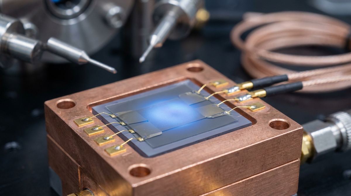
Introduction to ESR-Driven Photogalvanics
In high-frequency electronics and quantum sensing, detecting electron spin resonance (ESR) typically requires bulky microwave cavities and complex detection setups. However, recent research has demonstrated that monolayer graphene and graphene-based heterostructures can convert microwave radiation directly into a measurable DC voltage through the linear photogalvanic effect (LPGE).
This phenomenon occurs when linearly polarized microwave radiation (specifically in the 45-75 GHz range) interacts with the electron spins in the graphene lattice. This interaction creates a resonant photocurrent that is highly sensitive to the magnetic field orientation and the charge-carrier density. For an engineer or a small lab, this means you can build a micron-scale sensor that acts as a probe for spin states, effectively turning a simple graphene device into a high-frequency microwave detector.
The Application: High-Frequency Spin Characterization
The primary application for this technology is the development of ultra-compact, high-frequency spin-state sensors. Unlike traditional ESR equipment, which is often limited by the size of the resonant cavity, a graphene-based photogalvanic sensor can be integrated directly into a circuit.
This makes it useful for:
1. Characterizing spin properties in semiconductor heterostructures.
2. Developing high-frequency microwave detectors for 60 GHz communication bands.
3. Testing spin-based logic components in quantum computing prototypes.
By measuring the DC voltage produced by the device, you can determine the exact frequency and magnetic field conditions required for spin resonance, providing a direct readout of the spin environment without needing to intercept the microwave signal itself.
Required Materials and Components
To build a prototype of this sensor, you will need high-quality 2D materials and precision fabrication equipment.
1. Monolayer Graphene: High-mobility graphene is essential. CVD-grown graphene is acceptable for prototyping, but exfoliated graphene is preferred for high-performance testing.
2. WSe2 (Tungsten Diselenide): A monolayer or few-layer WSe2 layer is used to create a heterostructure. The WSe2 provides the necessary interaction to enhance the signal.
3. Substrate: Hexagonal Boron Nitride (hBN) is highly recommended as a substrate or encapsulation layer to maintain high carrier mobility. A silicon/silicon dioxide (Si/SiO2) substrate can be used for simpler, less sensitive prototypes.
4. Electrodes: Gold (Au) and Titanium (Ti) for contact pads.
5. Microwave Source: A signal generator capable of producing 45-75 GHz radiation.
6. Magnetic Field Source: An electromagnet or a superconducting magnet capable of providing both in-plane (Voigt geometry) and out-of-plane (Faraday geometry) magnetic fields.
7. Measurement Electronics: A high-sensitivity lock-in amplifier and a low-noise DC voltage source.
Prototype Construction Steps
Building this device requires cleanroom facilities for micro-fabrication.
1. Substrate Preparation: Clean your Si/SiO2 or hBN substrate using standard RCA cleaning procedures to ensure no organic residue remains.
2. Heterostructure Assembly: Use a dry-transfer technique (such as the PC or PDMS method) to stack the layers. The recommended stack is Substrate / hBN / WSe2 / Graphene / hBN. The alignment between the WSe2 and graphene layers is critical for maximizing the spin-orbit coupling effects.
3. Device Patterning: Use electron-beam lithography (EBL) to define the channel area and the contact pads. For a micron-scale device, aim for a channel length of approximately 10 to 50 micrometers.
4. Electrode Deposition: Deposit Ti/Au contacts via thermal evaporation. The Ti layer ensures good adhesion, while the Au layer provides low contact resistance.
5. Encapsulation: If not already done during the transfer process, encapsulate the device with a final layer of hBN to protect it from environmental degradation and reduce charge noise.
6. Microwave Coupling: Integrate the device into a microwave setup. This can be achieved by placing the device in a specialized microwave probe station or by using a micro-antenna structure fabricated near the device to couple the 45-75 GHz radiation into the graphene layer.
Testing and Calibration Plan
Once the device is fabricated, follow this testing sequence to validate the ESR-driven photogalvanic effect.
1. DC Characterization: Apply a gate voltage to the device and measure the resistance/conductance. Identify the charge-neutrality point (Dirac point) where the resistance is at its maximum.
2. Microwave Excitation: Apply linearly polarized microwave radiation in the 45-75 GHz range.
3. Magnetic Field Sweep: Apply a magnetic field and sweep it across a range of 0 to 1 Tesla. You should observe resonant features in the DC voltage as the magnetic field matches the ESR condition.
4. Geometry Verification:
- Faraday Geometry: Apply the magnetic field perpendicular to the plane of the graphene.
- Voigt Geometry: Apply the magnetic field parallel to the plane of the graphene.
The resonant features should be present in both, but their characteristics may differ.
5. Sign Reversal Test: This is the most critical validation step. As you sweep the gate voltage through the charge-neutrality point, the sign of the resonant photocurrent must reverse. This confirms that the signal is due to the photogalvanic effect and not just simple heating (bolometric effect).
Engineering Assumptions and Parameters
Since this is a specialized research-based application, the following parameters are proposed as cautious starting points for an engineering prototype:
- Channel Dimensions: 20 micrometers length by 1 micrometer width.
- Microwave Frequency: Start at 50 GHz and sweep toward 75 GHz.
- Magnetic Field Strength: 0.5 Tesla is a sufficient starting point for many spin-resonance observations.
- Temperature: While the research suggests these effects can be observed at room temperature, for a reliable prototype, testing at 77K (Liquid Nitrogen) is recommended to reduce thermal noise and increase carrier mobility.
- Microwave Power: Start with very low power (microwatts) to avoid sample heating, which can mask the photogalvanic signal.
Risks and Mitigation
1. Contact Resistance: High contact resistance can drown out the small photogalvanic signal. Mitigation: Use optimized Ti/Au deposition and ensure the graphene is properly encapsulated to prevent oxidation at the contact interface.
2. Thermal Effects: Microwave radiation can cause Joule heating, creating a bolometric signal that mimics the photogalvanic effect. Mitigation: Use the sign-reversal test at the charge-neutrality point to distinguish the two. The photogalvanic signal changes sign, while the thermal signal does not.
3. Signal-to-Noise Ratio (SNR): The resonant photocurrent is extremely small. Mitigation: Use a lock-in amplifier synchronized with the microwave source or a modulated magnetic field to extract the signal from the noise.
4. Layer Alignment: Misalignment of the WSe2 and graphene layers can significantly reduce the signal. Mitigation: Use high-precision optical or electron-microscope alignment during the dry-transfer process.
Source Basis
This guide is based on the research findings presented in:
Bray, C., et al. (2026). Electron spin resonance driven photogalvanic effect in graphene-based structures. arXiv:2608.26026v1.
The implementation of this device relies on the microscopic theory that radiation-induced momentum alignment followed by skew scattering generates the observed resonant photocurrent.