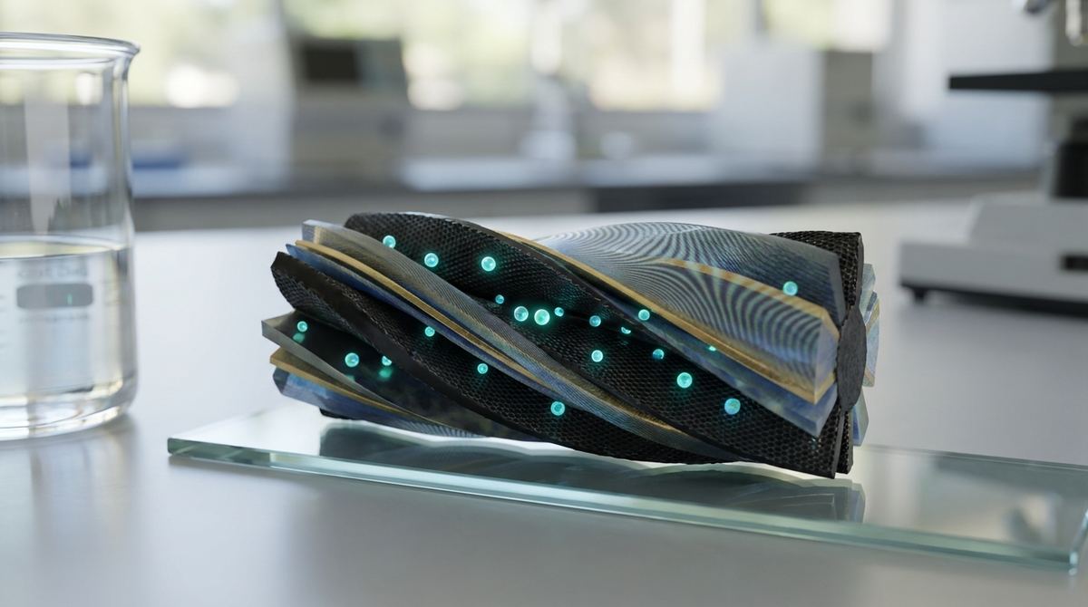
Imagine a world where the devices we use every day, from the sensors in our smartphones to the solar panels on our roofs, are exponentially more efficient because we learned how to manipulate matter by simply rotating it. In the realm of quantum materials, the way layers of atoms are stacked is not just a matter of structural organization, but a fundamental way to control the flow of electricity. By twisting one layer of atoms against another, scientists can create entirely new physical properties that do not exist in either material alone. This concept, often referred to as twistronics, is now opening doors to understanding how we can capture and move electrical charges with unprecedented speed and precision.
The Problem This Research Is Solving
In the pursuit of efficient energy harvesting and high-speed electronics, the fundamental enemy is a process called charge recombination. When light hits a semiconductor material, such as tungsten disulfide (WS2), it imparts energy to electrons, kicking them into a higher energy state and leaving behind a positive charge known as a hole. To create useful electricity or an electronic signal, these electrons and holes must be separated and moved toward electrodes before they can find each other and recombine. When they recombine, the energy they carried is lost as heat, resulting in a loss of efficiency in solar cells, photodetectors, and sensors.
The challenge for engineers is to find a way to facilitate the movement of electrons away from their corresponding holes as quickly as possible. If the electron can be handed off to a secondary material, like graphene, in a matter of femtoseconds, the chance of recombination is drastically reduced. However, the interface between two different materials is rarely perfect. The electronic properties at the junction where two different crystals meet are highly sensitive to how they are aligned. If the atoms of the two materials do not line up in a specific way, the electrical coupling between them may be weak, making the charge transfer slow and inefficient. Scientists have long struggled to find a reliable way to tune this interface to achieve the optimal speed for charge separation.
The Key Idea in Plain English
The solution suggested by recent academic inquiry lies in the geometric relationship between the overlapping layers, specifically known as the twist angle. When two identical or similar crystalline lattices are stacked, they naturally align in a way that repeats its pattern over a much larger distance than the individual atoms. This new, larger pattern is called a moiré superlattice. Think of it like placing two fine-mesh screens on top of one another; if they are perfectly aligned, the pattern is simple, but if you rotate one slightly, a complex, undulating pattern emerges across the surface.
This moiré pattern is not just a visual curiosity; it fundamentally changes the landscape that electrons see as they move through the material. By precisely controlling the twist angle between a layer of WS2 and a layer of graphene, researchers can manipulate the electronic landscape. This manipulation can create specific pathways or energy levels that act like a fast-lane for electrons. The goal is to find the "sweet spot" in the rotation where the electronic connection between the semiconductor and the graphene is at its most efficient, allowing electrons to jump from the WS2 to the graphene at an ultrafast pace, effectively outrunning the recombination process.
How the Graphene-Based System Works
To understand this system, we must look at the specific roles played by each component. WS2 is a transition metal dichalcogenide, a class of materials that are semiconductors. In its monolayer form, WS2 is particularly interesting because it possesses a direct bandgap, meaning it is exceptionally good at absorbing light and creating charge carriers. It acts as the primary harvester in this heterostructure, catching incoming photons and generating the electron-hole pairs necessary for electrical activity.
Graphene, on the other hand, is a single layer of carbon atoms arranged in a hexagonal lattice. It is a semimetal with extraordinary electron mobility, meaning electrons can travel through it with almost no resistance. In this heterostructure, graphene acts as the electron highway. The goal of the architecture is to ensure that once an electron is excited in the WS2, it immediately transitions into the graphene layer.
The interaction between these two materials is governed by the interface. When the WS2 is placed on the graphene, the electronic wavefunctions of both materials begin to overlap. This overlap is what allows for charge transfer. However, the nature of this overlap is dictated by the alignment of the atomic lattices. Because the hexagonal lattice of WS2 and the hexagonal lattice of graphene have different dimensions and symmetries, rotating them creates the moiré pattern. This pattern modifies the electronic band structure of the interface, effectively changing the energy barriers that an electron must cross to move from the semiconductor to the graphene.
What the Researchers Found
In a study conducted by Niklas Hofmann, Leonard Weigl, Johannes Gradl, Stiven Forti, Domenica Convertino, Camilla Coletti, and Isabella Gierz, the team investigated how these twist angles influence the speed and efficiency of this charge separation. Using advanced ultrafast spectroscopy, they were able to observe the movement of electrons on a timescale of quadrillionths of a second. The researchers focused on the ultrafast charge separation that occurs at the interface of the WS2-graphene heterostructure.
The findings revealed that the twist angle is a decisive factor in the kinetics of charge transfer. The study demonstrated that the rate at which electrons move from the WS2 into the graphene is not constant but is highly dependent on the relative orientation of the two lattices. By adjusting the angle, the researchers could observe changes in how quickly the charge separation occurs. This suggests that the moiré superlattice created by the twist angle creates a periodic modulation of the electronic potential, which can either facilitate or hinder the movement of electrons depending on the specific geometry. This discovery provides a roadmap for how to engineer these interfaces by selecting a specific twist angle that maximizes the speed of charge separation, ensuring that electrons are moved away from holes before recombination can occur.
Why the Result Matters
The implications of this research are profound for the field of condensed matter physics and materials science. First, it proves that the twist angle is a functional tool that can be used to tune the properties of a device. Instead of searching for entirely new materials, engineers can potentially use the same materials but achieve vastly different performance levels simply by altering their orientation. This adds a new dimension of control to material design.
Furthermore, the ability to achieve ultrafast charge separation is critical for the next generation of optoelectronic devices. For example, in high-speed photodetectors, the speed at which a device can respond to a light signal is limited by how fast the charge carriers can be separated. If we can use twistronics to optimize this process, we could create sensors that operate at much higher frequencies, enabling faster communication technologies. Similarly, in the realm of photovoltaics and photocatalysis, increasing the speed of charge separation directly translates to higher energy conversion efficiency, making renewable energy technologies more viable and powerful.
Limitations and What Still Needs Testing
While these findings are significant, it is important to recognize that this research is currently focused on fundamental physics and highly controlled laboratory environments. The study demonstrates how the twist angle influences charge separation at a microscopic level, but translating this to industrial-scale manufacturing presents massive challenges.
One major limitation is the precision required to maintain a consistent twist angle across a large area. Currently, most research in this field involves using mechanical exfoliation, where a thin flake of material is transferred onto another. This method is excellent for studying single, perfect flakes in a laboratory, but it is not a scalable manufacturing process. Producing large-area heterostructures where every single flake is rotated at the exact same angle is an engineering hurdle that has yet to be overcome.
Additionally, while the study identifies the importance of the angle, more work is needed to map out the complete landscape of these effects. Scientists need to determine exactly which angles yield the best results across different material combinations and under different environmental conditions, such as varying temperatures or the presence of moisture. There is also the question of how defects in the crystal structure might interact with the moiré pattern, potentially complicating the predictable behavior of the electrons.
Real-World Applications
The potential real-world applications for optimized WS2-graphene heterostructures are vast and diverse. In the field of telecommunications, the development of ultra-fast photodetectors could lead to much higher bandwidths in optical fiber networks, supporting the massive data demands of modern digital infrastructure. These detectors would be able to respond to light pulses with incredible speed, reducing signal latency.
In the energy sector, these materials could be used to create highly efficient photocatalysts. Photocatalysis is a process where light is used to trigger chemical reactions, such as the splitting of water into hydrogen and oxygen. Hydrogen is a clean-burning fuel of the future, and finding ways to produce it efficiently using sunlight is a holy grail of green chemistry. By optimizing the charge separation in a WS2-graphene system, we could maximize the efficiency of the chemical reactions driven by light.
Furthermore, the semiconductor industry could benefit from more efficient light-emitting diodes (LEDs) and advanced transistors. As we approach the physical limits of traditional silicon-based electronics, the ability to engineer new properties through twistronics offers a new frontier for high-performance computing and low-power mobile devices.
If You Remember One Thing
If there is one takeaway from this research, it is that the geometry of atoms is just as important as the atoms themselves; by rotating the way materials are stacked, we can control the speed of electricity at the most fundamental level.
FAQ
What is WS2 and why is it used in this research?
WS2, or tungsten disulfide, is a semiconductor material belonging to a class called transition metal dichalcogenides. It is used in these studies because it is very efficient at absorbing light and generating electrical charges, making it an ideal candidate for the first layer in a light-sensitive device.
Why is graphene so important in these heterostructures?
Graphene is a single layer of carbon atoms known for its incredible ability to conduct electricity. In this specific research, graphene acts as an electron highway, pulling electrons away from the WS2 layer so that they can be used as electrical current or used in a chemical reaction.
What exactly is a twist angle in this context?
A twist angle refers to the specific degree of rotation between two layers of materials as they are stacked together. Even a tiny change in this angle can completely change how the atoms of the two layers interact, which in turn changes how electrons move between them.
How does rotating a layer change the behavior of electricity?
When you rotate one layer, you create a moiré pattern, which is a new, larger pattern created by the overlapping grids of atoms. This pattern changes the energy landscape that electrons experience, essentially creating new "paths" or "barriers" that dictate how fast and in what direction the electrons can move.
Is this technology ready to be used in everyday electronics?
Not yet. While the research provides essential scientific insights into how these materials behave, there is still a significant gap between laboratory-scale experiments and mass-market manufacturing. Challenges remain in creating large, perfectly aligned sheets of these materials for use in commercial products.
Conclusion
The research conducted by Hofmann, Weigl, Gradl, Forti, Convertino, Coletti, and Gierz marks a significant step forward in our ability to engineer the quantum landscape. By demonstrating that the twist angle is a powerful lever for controlling ultrafast charge separation in WS2-graphene heterostructures, they have provided a new tool for the design of next-generation materials. As we move from understanding these atomic rotations to mastering them in industrial manufacturing, the ability to tune the fundamental properties of light and electricity through geometry may become a cornerstone of future technology.