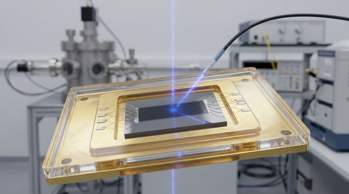
The Terahertz Gap and the Graphene Solution
Terahertz (THz) radiation occupies the frequency spectrum between microwaves and infrared light. For decades, this region has been known as the THz gap because it is notoriously difficult to detect and generate. Traditional THz detectors often rely on semiconductor P-N junctions, such as Schottky diodes. While effective, these junctions face fundamental physical limits regarding speed, sensitivity, and the requirement for cryogenic cooling in many high-performance scenarios.
Recent research has identified a way to bypass the need for a physical junction entirely. By using the Nonlinear Hall Effect (NLHE) in bilayer graphene, we can create a junction-free rectifier. In this process, the material itself breaks inversion symmetry to convert THz electromagnetic waves directly into a measurable DC voltage. The breakthrough reported by Melegari et al. (2026) shows that by using double-ionic gating, we can achieve a nonlinear susceptibility that is orders of magnitude larger than previous room-temperature attempts, making this a viable path for commercial-grade THz sensing.
The Engineering Objective: A Junction-Free THz Rectifier
The goal for an engineer or startup is to build a device that exhibits high THz voltage responsivity at room temperature. The research indicates a responsivity of approximately 4 x 10^4 V/W. This is comparable to commercial Schottky diodes but offers the advantage of being junction-free, which potentially allows for much faster response times and easier integration into CMOS-compatible processes.
The core mechanism relies on the ability to tune the inversion symmetry of the bilayer graphene. By applying different voltages to the top and bottom gates, you can control the Berry curvature and the nonlinear susceptibility. This allows you to not only detect the signal but also switch the signal on, off, or even reverse its polarity—a feature critical for advanced signal processing and noise reduction.
Required Materials and Hardware
To prototype this device, you will need high-quality graphene and precise gating capabilities. Because the effect relies on high carrier mobility, standard CVD graphene may be insufficient; hBN-encapsulated graphene is the preferred standard for lab-scale prototyping.
1. Bilayer Graphene: Ideally exfoliated bilayer graphene encapsulated between two layers of hexagonal Boron Nitride (hBN).
2. Substrate: Silicon/Silicon Dioxide (Si/SiO2) substrate, which serves as the back gate.
3. Gating Medium: Ionic liquid (such as DEME-TFSI) or a solid-state electrolyte. This is required to achieve the high capacitance needed for strong inversion breaking.
4. Electrodes: Gold (Au) for contacts, with a thin Titanium (Ti) or Chromium (Cr) adhesion layer.
5. Lithography Equipment: Electron Beam Lithography (EBL) system for defining fine-scale contact patterns.
6. THz Source: A femtosecond laser coupled with a photoconductive antenna or a THz-TDS (Time-Domain Spectroscopy) setup.
7. Measurement Hardware: A lock-in amplifier and a high-impedance pre-amplifier to detect the small DC voltage generated by the THz pulse.
Prototype Construction Steps
Building this device requires a standard microfabrication workflow with a specific focus on the dual-gate architecture.
1. Substrate Preparation: Clean a Si/SiO2 substrate using standard RCA cleaning or a piranha etch to ensure a pristine surface for flake deposition.
2. Graphene/hBN Assembly: Using a dry transfer method (such as the PMMA-assisted method), stack the layers in the following order: Bottom hBN, Bilayer Graphene, and Top hBN. This sandwich structure is critical to protect the graphene and maintain high mobility.
3. Contact Patterning: Use Electron Beam Lithography to define the contact pads. Perform metal evaporation (Ti/Au) to create the source and drain electrodes.
4. Ionic Gate Integration: This is the most critical step for achieving the nonlinear Hall effect. You must apply an electrolyte over the device. For a lab prototype, an ionic liquid can be dropped onto the top hBN layer. For a more stable, device-ready version, a solid-state electrolyte (like a polymer-based ion conductor) should be spin-coated over the device.
5. Gate Electrode Setup: The bottom gate is the Si substrate itself. The top gate is the electrode used to apply voltage to the ionic liquid/electrolyte layer.
The Testing and Validation Protocol
Once the device is fabricated, you must verify the nonlinear Hall response and the switchability of the signal.
1. DC Characterization: Before applying THz radiation, perform standard I-V (current-voltage) measurements to ensure the device is Ohmic and the graphene mobility is within the expected range (aim for >10,000 cm2/Vs at room temperature).
2. THz Response Measurement: Direct a pulsed THz beam at the device. Use the lock-in amplifier, synchronized with the THz pulse trigger, to measure the resulting DC voltage (V_NLHE).
3. Responsivity Calculation: Calculate the responsivity (V/W) by measuring the THz power (W) incident on the device. Compare this to the target value of 4 x 10^4 V/W.
4. Symmetry Switching Test: This is the most important validation of the research. Vary the top gate voltage (V_top) and the bottom gate voltage (V_bottom) independently. You should observe the DC voltage signal changing from positive to negative as you cross the point where inversion symmetry is restored. This confirms the switchable nature of the device.
Engineering Risks and Mitigation
While the physics is robust, several engineering challenges must be addressed before this can move from a lab prototype to a commercial product.
1. Electrochemical Stability: Ionic liquids can undergo electrolysis if the voltage exceeds the electrochemical window. This can degrade the graphene or the hBN.
- Mitigation: Use electrolytes with a wide electrochemical window and strictly monitor the gate voltage limits.
2. Contact Resistance: High contact resistance can mask the nonlinear signal.
- Mitigation: Use EBL for precise contact placement and optimize the metal-graphene interface through thermal annealing.
3. Signal-to-Noise Ratio (SNR): The generated DC voltage is very small.
- Mitigation: Use high-impedance, low-noise pre-amplifiers and lock-in detection to extract the signal from the thermal noise.
4. Device Uniformity: Maintaining a consistent bilayer thickness across a large area is difficult with exfoliated flakes.
- Mitigation: For scaling, transition to high-quality CVD bilayer graphene grown on copper and transferred to hBN.
Source Basis
This guide is based on the research findings of Melegari et al. (2026) regarding the giant room-temperature nonlinear Hall effect in double-ionic gated bilayer graphene. The responsivity values and the mechanism of inversion symmetry breaking via dual gating are derived directly from the reported experimental data. Engineering assumptions regarding the use of hBN encapsulation and specific electrolyte types are provided to facilitate practical implementation.