Graphene is often celebrated as a miracle material due to its extraordinary conductivity and strength, yet it possesses a fundamental flaw that prevents it from replacing silicon in our modern computers. In the digital world, everything relies on the ability to switch an electrical current on and off, much like a light switch. Silicon works because it has a band gap, a specific energy barrier that prevents electrons from flowing unless a certain amount of voltage is applied. Graphene, however, is a semimetal with no band gap, meaning it is always on. This research provides a theoretical blueprint for how we might finally fix this, turning graphene from a simple conductor into a sophisticated semiconductor that could power the next generation of superfast electronics.
This breakthrough in material science was explored through the rigorous theoretical work of Diyan Unmu Dzujah, Hongde Yu, and Thomas Heine. By studying how specific patterns of missing electrons can be used to manipulate the electronic structure of graphene, these researchers have provided a roadmap for engineers to create graphene superlattices with precisely controlled properties.
The Problem This Research Is Solving
To understand the importance of this research, one must first understand the limitations of current semiconductor technology and the specific challenge graphene presents. Modern computing is built upon the transistor, a tiny switch that controls the flow of electricity. For a transistor to be effective, it must have a clear distinction between its on-state and its off-state. This distinction is provided by the band gap. In a semiconductor, the band gap is a range of energy levels where electrons are not allowed to exist. When the energy provided to the material is lower than the band gap, the material acts as an insulator, effectively turning the current off.
Graphene, the single layer of carbon atoms arranged in a honeycomb lattice, is incredibly fast because its electrons behave as if they have no mass, moving with unprecedented speed. However, because graphene lacks a band gap, it cannot be effectively turned off. If you attempt to use graphene in a standard digital logic circuit, the current will continue to leak through the material even when the transistor is supposed to be in the off-state. This leakage leads to massive power consumption and heat generation, making it impossible to pack billions of graphene transistors into a single microchip like we do with silicon. Therefore, the "holy grail" of graphene research is to find a way to open a band gap without destroying the material's exceptional electrical mobility.
The Key Idea in Plain English
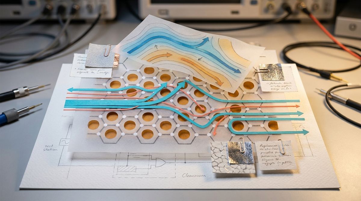
The researchers propose a solution that involves creating a superlattice. To understand a superlattice, imagine a very regular, repeating pattern of something added to a base material. In this case, the base material is the perfect, uninterrupted honeycomb lattice of graphene. The addition is a periodic distribution of π-vacancies.
A π-vacancy is essentially a "hole" in the electronic structure. While a structural vacancy means an entire carbon atom is missing from the lattice, a π-vacancy refers to a location where the electron density—specifically the electrons that participate in the chemical bonding that allows electricity to flow—is disrupted. By arranging these vacancies in a perfectly repeating, periodic pattern across the graphene sheet, you create a new, larger structural pattern called a superlattice. This new pattern changes how electrons move through the material. It creates a new set of energy rules for the electrons, effectively building the "wall" or the band gap that was previously missing.
How the Graphene-Based System Works
To explain the mechanism, we must look at the atomic geometry of graphene. Graphene is composed of two interlocking triangular sublattices, often referred to as the A and B sublattices. In pristine graphene, these two sublattices are identical in their electronic properties. This symmetry between the A and B sublattices is the direct cause of the zero-band-gap nature of the material. Because the sublattices are perfectly balanced, the electronic wavefunctions of the electrons can cross each other at a single point, known as the Dirac point, without any energy barrier.
The research by Diyan Unmu Dzujah, Hongde Yu, and Thomas Heine focuses on breaking this sublattice symmetry. When you introduce a vacancy, you are essentially removing a site that was once part of one of these sublattices. This creates an imbalance. If you place these vacancies in a periodic fashion, you are no longer dealing with a simple honeycomb lattice. Instead, you are creating a "superlattice" where the unit cell of the material has become much larger than the original single carbon atom cell.
The cause and effect relationship here is rooted in the physics of wave interference. As electrons move through the graphene lattice, they behave like waves. When they encounter a periodic array of vacancies, they undergo a phenomenon similar to Bragg scattering. The periodic arrangement of these π-vacancies creates a new potential landscape. This landscape forces the electron wavefunctions to reorganize. As the wavefunctions reorganize to accommodate the new periodic potential, a gap is forced open at the Dirac point. The size and shape of this gap are directly determined by the density and the specific geometric arrangement of the vacancies. By controlling the "pattern" of the holes, scientists can theoretically "tune" the band gap to the exact energy level required for a specific electronic application.
What the Researchers Found
The researchers provided a set of guidelines for how to achieve this band gap opening most effectively. Their findings suggest that not all patterns of vacancies are created equal. The ability to open a significant band gap depends heavily on the symmetry and the spatial distribution of the π-vacancies.
They discovered that by carefully selecting the periodicity of the vacancies, it is possible to manipulate the electronic dispersion relations—the mathematical description of how an electron's energy relates to its momentum. Specifically, the research outlines how different superlattice geometries can lead to different electronic outcomes. Some patterns might result in a small, narrow gap, while others might create a much wider, more robust gap. This is crucial because a larger band gap allows the material to operate at higher temperatures without the electrons accidentally jumping the gap due to thermal energy, which would cause the transistor to fail.
Importantly, the research emphasizes that the distribution of these vacancies does not necessarily require the physical removal of carbon atoms. The study suggests that the electronic effect can be achieved through π-vacancies, which are more about the distribution of the electron density itself. This opens up much more possibilities for manufacturing, as it is often easier to manipulate electron density through chemical doping or specialized light exposure than it is to physically remove atoms from a lattice one by one.
Why the Result Matters
The implications of these findings are profound for the future of semiconductor physics. If we can master the ability to create these superlattices, we solve the single biggest hurdle to graphene-based digital logic. By transforming graphene from a semimetal into a controllable semiconductor, we enable a new class of high-speed, low-power electronics.
The ability to tune the band gap via vacancy distribution means that a single material—graphene—could potentially be used for a variety of different tasks. One specific pattern of vacancies could be used for high-speed digital processors, while a different pattern could be optimized for optoelectronics, such as highly sensitive light detectors or emitters. This versatility is something that silicon, which has a fixed band gap, cannot easily match. The ability to engineer the electronic properties of a material through structural and electronic design represents a fundamental shift from "using" materials to "programming" materials.
Limitations and What Still Needs Testing
While the theoretical guidelines provided by Diyan Unmu Dzujah, Hongde Yu, and Thomas Heine are a massive step forward, there are significant engineering challenges that remain. The primary limitation is the precision of manufacturing. Creating a perfectly periodic pattern of vacancies at the atomic scale is an immense technical challenge. Current lithography techniques are not precise enough to place individual vacancies or dopant atoms in the exact, repeating geometric patterns required to create a controlled superlattice.
Furthermore, the stability of these vacancy patterns is a major concern. In a real-world device, atoms and electrons are in constant motion due to heat and external electrical fields. There is a risk that the periodic pattern of vacancies could migrate or heal over time, which would cause the band gap to vanish or change, rendering the device useless. Future research must focus on how to "lock" these vacancy patterns into place to ensure long-term reliability. Additionally, the electrical mobility of the electrons—the very thing that makes graphene great—might be reduced by the presence of these vacancies. If the vacancies scatter the electrons too much, the material might become a semiconductor, but it will be a slow one. Finding the "sweet spot" where the band gap is large enough to be useful but the electron speed remains high is the next great frontier.
Real-World Applications
The successful implementation of graphene superlattices would trigger a revolution across several industries. In the consumer electronics sector, we could see the birth of ultra-fast processors that consume a fraction of the power of current silicon chips, leading to smartphones and laptops with vastly improved battery life and performance.
In the field of sensing, these superlattices could create highly sensitive chemical or biological sensors. Because the electronic properties of the superlattice are so sensitive to the presence of other molecules, a single molecule landing on the surface could cause a measurable change in the band gap, allowing for the detection of toxins or disease markers at extremely low concentrations.
Optoelectronics is another major frontier. The ability to tune the band gap means we can design graphene-based components that respond to specific wavelengths of light. This could lead to new types of high-speed optical communication systems, where light and electricity are seamlessly integrated on a single chip, enabling much faster data transfer for the global internet infrastructure.
If You Remember One Thing
If you take away only one concept from this research, let it be this: Graphene's potential for digital computing is unlocked not by keeping its structure perfect, but by introducing a perfectly ordered pattern of imperfections. By breaking the symmetry of the carbon lattice through periodic vacancies, we can create the band gap necessary to turn graphene from a simple conductor into the world's most advanced semiconductor.
FAQ
Question: What exactly is a band gap and why is it important?
Answer: A band gap is an energy range in a material where no electrons can exist. It acts as a barrier that determines whether a material conducts electricity or acts as an insulator. For digital electronics, a band gap is essential because it allows us to turn a transistor "off" by preventing current from flowing when it is not needed.
Question: Why does graphene not have a band gap naturally?
Answer: Graphene is composed of two identical sublattices that are perfectly balanced in their electronic properties. This symmetry allows electrons to move through the material without encountering an energy barrier, meaning there is no gap to stop the flow of electricity, making the material a semimetal rather than a semiconductor.
Question: What is the difference between a structural vacancy and a π-vacancy?
Answer: A structural vacancy occurs when a physical atom is removed from the graphene lattice, creating a hole in the structure. A π-vacancy refers to a disruption in the electron density—specifically the electrons in the pi-orbitals—which can change the electronic properties of the material without necessarily requiring the removal of an entire atom.
Question: What is a superlattice in the context of this research?
Answer: A superlattice is a new, larger repeating pattern created when a base material, like graphene, is modified by a periodic arrangement of defects or atoms. This new, larger pattern changes the fundamental electronic rules of the material, allowing for the creation of new energy gaps.
Question: Can we use this technology in our phones today?
Answer: No, this research is currently theoretical and focuses on the guidelines for how such a system should be designed. While it provides a roadmap for the future, we still face major engineering hurdles in manufacturing these atomic patterns with the precision and stability required for commercial electronics.
Conclusion
This research points toward a practical lesson: graphene-based materials are most powerful when their nanoscale properties are connected to a clear engineering problem. The result is not a finished commercial product by itself, but it gives researchers and manufacturers a better map for designing lighter, more sensitive, or more durable systems. Future work still needs testing under real operating conditions, but the direction is promising because it joins materials science with application-driven design.