
AI Designs Graphene Nanocomposite for Interstellar Spacecraft Shielding
Researchers use AI to accelerate the discovery of new materials, identifying a graphene-boron nitride composite for interstellar spacecraft shielding.
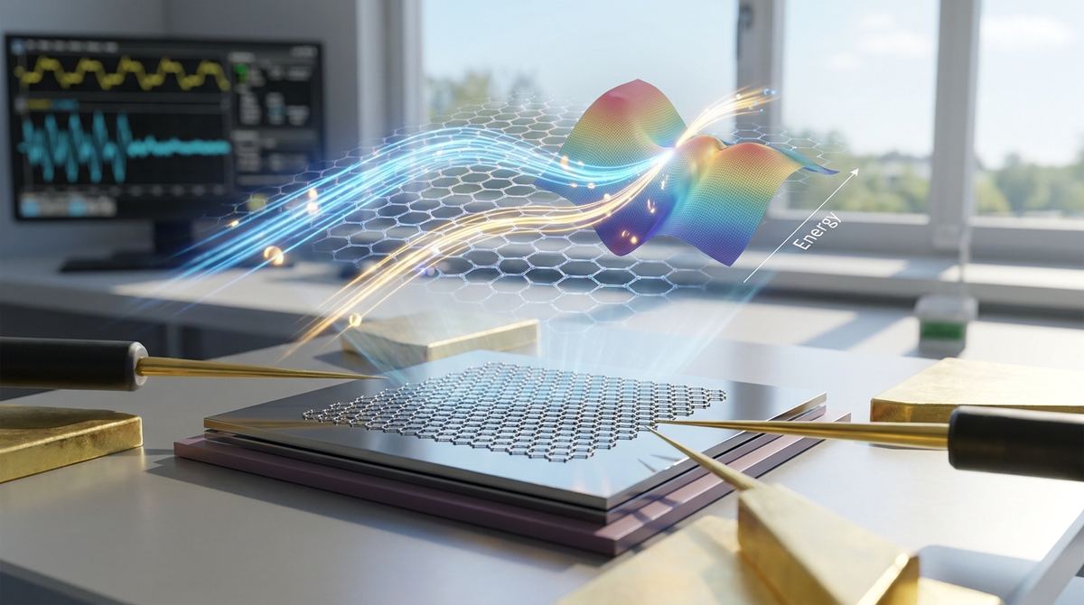
Imagine a computer that processes information much like a human brain does. In your own brain, the neurons that perform calculations and the synapses that store memories are essentially the same thing. Information is stored exactly where it is processed, allowing for nearly instantaneous reaction and incredible energy efficiency. Modern computers, however, do not work this way. They rely on a separation between where data is stored and where it is calculated, a design that creates a massive energy and speed barrier. As we reach the physical limits of traditional silicon technology, scientists are looking toward the world of two-dimensional materials to break this barrier. This transition represents a fundamental shift in how we build the machines of the future, moving away from rigid, linear processing and toward something much more fluid and efficient.
To understand why new materials are necessary, we must first understand the fundamental flaw in current computing architecture, known as the von Neumann bottleneck. Since the mid-twentieth century, almost every computer has used the von Neumann architecture, which separates the central processing unit, or CPU, from the memory unit. The CPU performs the logic and arithmetic, while the memory holds the instructions and the data. For the computer to do anything, it must constantly move data back and forth between these two distinct locations via a communication bus.
As we demand more power for artificial intelligence and complex simulations, this movement of data becomes the primary limiting factor. The bus has a limited bandwidth, meaning it can only carry so much information at once, and the energy required to move data across these physical distances is much higher than the energy required to actually compute it. This results in a massive waste of electricity and a ceiling on how fast a processor can actually operate. We are essentially trying to run a high-speed racing car through a narrow, congested tunnel. Even if the engine is incredibly powerful, the speed is limited by the tunnel's width. As transistors shrink to the atomic scale, silicon faces additional challenges, including increased heat generation and quantum tunneling, where electrons leak through barriers they are supposed to be contained by.
The perspective provided by Yaser Banad suggests that the solution lies in moving away from this separation. Instead of having a separate brain and memory, we need a system where the memory and the processing are integrated into a single, cohesive unit. This is often referred to as in-memory computing or neuromorphic computing. In these systems, the material itself acts as both the storage device and the processing element.
Two-dimensional materials, such as graphene and other atomically thin layers, offer a unique way to achieve this. Because these materials are only one or a few atoms thick, they can be layered or stacked in ways that are impossible with bulk materials like silicon. This extreme thinness allows us to control electrical signals with incredible precision using electric fields. By manipulating the properties of these layers, we can create components that mimic the behavior of biological synapses, which can strengthen or weaken their connections based on the amount of electrical charge that passes through them. This allows the hardware to learn and adapt, much like a biological brain, without needing to move data across a bus.
The functionality of these next-generation systems relies on the unique physics of two-dimensional lattices. Graphene, for example, is a single layer of carbon atoms arranged in a hexagonal pattern. This structure gives it extraordinary electrical properties. Because the layer is so thin, the electrons within it experience very little interference from the bulk material, leading to exceptionally high carrier mobility. This means that electrons can travel through the material at much higher speeds than they can in traditional silicon, which directly reduces the latency involved in signal transmission.
When we integrate graphene or other two-dimensional materials like transition metal dichalcogenides into a circuit, we can utilize their surface-to-volume ratio to our advantage. In a 2D material, every single atom is on the surface. This means that the electronic state of the material is incredibly sensitive to external influences, such as an electric field applied through a gate electrode. By applying a voltage, we can change the density of charge carriers in the material, effectively turning the material's resistance up or down.
In a neuromorphic context, this sensitivity allows us to create memristors. A memristor is a component that remembers its resistance state even after the power is turned off. In a 2D material-based memristor, the movement of ions or the shifting of charge within the atomic layers changes the electrical resistance of the material. Because this resistance can be tuned to many different levels—not just a simple on or off—the material can represent a range of weights, much like the synaptic strength in a human brain. This ability to provide a continuous range of resistance is what enables the hardware to perform complex, brain-like calculations through analog signals rather than the binary ones used in traditional computers.
In this perspective, Yaser Banad outlines the landscape of how 2D materials are poised to revolutionize computing. The research indicates that we are moving toward a paradigm where the distinction between hardware and software becomes blurred through neuromorphic architectures. The study suggests that by using 2D materials, we can create highly scalable, low-power architectures that are specifically optimized for the heavy mathematical lifting required by artificial intelligence.
The analysis highlights that the integration of various 2D materials can provide a diverse toolkit for engineers. While graphene is excellent for its high conductivity and speed, it lacks a natural bandgap, which makes it difficult to use as a simple switch in traditional logic. However, by pairing graphene with other 2D materials that do have a bandgap, such as molybdenum disulfide, researchers can create hybrid systems that combine the high-speed transport of graphene with the precise switching capabilities of other materials. This combination allows for the creation of sophisticated, multi-functional devices that can handle both traditional logic and neuromorphic memory functions within the same atomic-scale footprint.
The implications of this research are profound for the future of technology. Currently, training a large-scale artificial intelligence model requires massive data centers that consume enormous amounts of electricity. Much of this energy is lost simply because data is being shuttled between memory and processors. If we can transition to 2D material-based in-memory computing, the energy efficiency of AI could increase by several orders of magnitude. This would make it possible to run highly advanced AI on tiny, battery-powered devices, such as drones, wearable medical sensors, or autonomous vehicles, without needing to connect to a massive cloud server.
Furthermore, the ability to scale these materials down to the atomic level means that we can continue to increase computing density long after silicon has reached its physical limits. As we move toward the era of edge computing, where processing happens locally on the device rather than in a central server, the efficiency and speed provided by 2D materials will be the deciding factor in how smart our everyday objects become. We are looking at a future where your glasses, your watch, and even your home appliances possess a level of integrated intelligence that is currently impossible with existing hardware.
Despite the immense potential, there are significant hurdles that must be overcome before 2D materials can replace silicon in commercial computers. One of the primary challenges is scalability and manufacturing consistency. While we can create perfect, single-layer graphene in a laboratory setting using specialized equipment, producing it in large, uniform sheets at a scale suitable for mass manufacturing is incredibly difficult. Any defect, even a single missing atom in the lattice, can significantly alter the electrical properties of the material, leading to unreliable computing components.
Another major engineering challenge is the contact resistance problem. When you try to connect a three-dimensional metal wire to a two-dimensional material, the interface often creates high electrical resistance. This resistance can negate the speed and efficiency benefits that the 2D material provides. Researchers are currently testing various ways to optimize these interfaces, such as using specialized buffer layers or different metal deposition techniques, but a standardized, high-yield method does not yet exist. Additionally, the long-term stability of these materials when exposed to oxygen and moisture in the air remains a concern, requiring advanced encapsulation techniques to ensure the devices function reliably over many years.
The application of 2D material-based computing will likely manifest first in specialized fields before moving into general-purpose computing. One immediate application is in the realm of edge artificial intelligence. Autonomous drones, which must make split-second decisions to avoid obstacles, would benefit immensely from the low-latency, high-efficiency processing provided by neuromorphic 2D chips. These drones could process visual data locally, reducing the need for a constant, high-bandwidth connection to a remote server.
Another significant application is in medical technology. Implantable devices, such as smart pacemakers or neural interfaces, require extreme energy efficiency to operate safely inside the human body for long periods. 2D material-based processors could provide the necessary computational power for real-time health monitoring while consuming a fraction of the power required by current microchips, significantly extending the lifespan of these life-saving devices. Finally, in the field of large-scale data centers, switching to in-memory computing could drastically reduce the carbon footprint of the global digital infrastructure by minimizing the energy wasted during data movement.
If you remember only one thing from this technical overview, let it be that the future of computing is not about making transistors smaller, but about making the architecture smarter by using the unique properties of two-dimensional materials to merge memory and processing into a single, efficient system.
How does a 2D material differ from a traditional material like silicon?
Traditional materials like silicon are three-dimensional, meaning their properties are determined by their bulk volume. In contrast, two-dimensional materials like graphene are only one or a few atoms thick. This extreme thinness means that every atom is on the surface, making the material incredibly sensitive to electric fields and allowing for much tighter control over how electrons move through the system.
What exactly is the von Neumann bottleneck?
The von Neumann bottleneck is a performance limitation caused by the physical separation of the processor and the memory in standard computers. Because data must travel back and forth between these two components through a relatively narrow pathway, the time and energy spent moving the data becomes a major barrier to computing speed and efficiency.
Why is graphene so special for electronics?
Graphene is famous for its extraordinary electrical conductivity. Because of its unique atomic structure, electrons can travel through it with very little resistance and at much higher speeds than in silicon. This high mobility is essential for creating faster, more efficient electronic components that can operate with minimal energy loss.
What is neuromorphic computing?
Neuromorphic computing is a method of designing computer hardware that mimics the structure and function of the human brain. Instead of using the traditional separation of memory and processing, neuromorphic systems use components like memristors that can both store and process information, allowing for highly efficient, brain-like computation.
Is this technology ready for use in my smartphone today?
No, the technology is still in the research and development phase. While there have been many successful laboratory demonstrations, scientists still need to figure out how to manufacture these 2D materials consistently at a massive scale and how to integrate them reliably with existing electronic systems without increasing electrical resistance or losing stability.
The transition from traditional von Neumann architectures to new, 2D material-based systems represents one of the most significant shifts in the history of computing. By leveraging the unique physics of atomically thin materials, researchers like Yaser Banad are paving the way for a future where computing is as efficient and integrated as the biological systems that inspired it. While challenges in manufacturing and integration remain, the potential for a revolution in artificial intelligence, edge computing, and energy efficiency makes this one of the most vital areas of modern scientific research.
Serious about B2B integration? Test our premium Pulsed Electrical Resistive Carbon Heating turbostratic graphene in your lab. 100g sample packs available now.
Explore More
Researchers use AI to accelerate the discovery of new materials, identifying a graphene-boron nitride composite for interstellar spacecraft shielding.

In BN-encapsulated graphene, the ultimate limit on electron speed is not graphene itself, but remote phonon scattering from the insulating layers that...

Determinant Monte Carlo simulations are key to materials science but fail at low temperatures. New research offers a stable algorithm, enabling accurate...