
Graphene’s Ultimate Speed Limit: The Boron Nitride Casing Is the Bottleneck
In BN-encapsulated graphene, the ultimate limit on electron speed is not graphene itself, but remote phonon scattering from the insulating layers that...
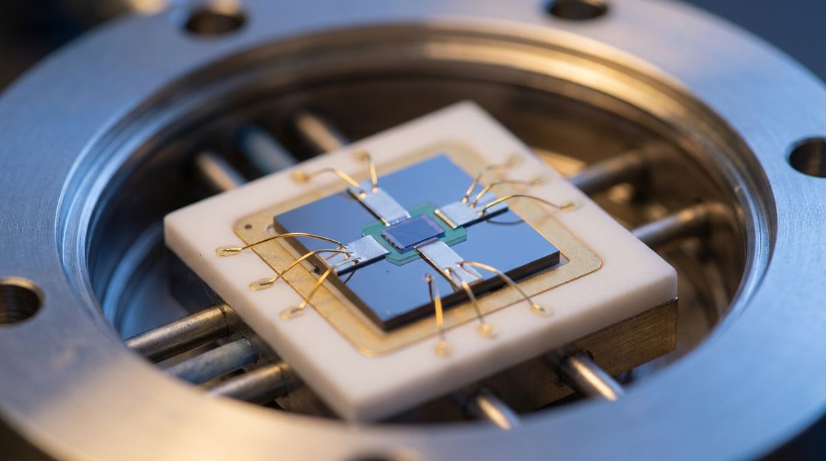
The recent research by Galante-Agero et al. (2026) demonstrates that bilayer graphene (BLG) can inherit superconductivity from a nearby aluminum electrode through the proximity effect. This phenomenon allows for the creation of a gate-defined quantum point contact (QPC) where the transport properties are governed by discrete one-dimensional modes. For an engineer or a startup specializing in quantum technologies, this represents a path toward creating a new class of cryogenic sensors.
Instead of relying on standard resistive changes, this sensor utilizes the discrete switching current of a superconducting-hybrid graphene channel. Because the switching current follows the underlying mode structure of the QPC, the device acts as a highly non-linear transducer. A minute change in the local environment—such as a fractional change in magnetic field, a tiny temperature fluctuation, or a single charge offset—can trigger a transition from the superconducting state to the normal state, resulting in a massive, measurable jump in conductance.
The goal is to build a device that operates in the ballistic transport regime, where electrons move through the graphene without scattering. By using a gate to narrow the graphene channel into a QPC, we force the electrons into specific one-dimensional modes.
When an aluminum electrode is placed in close proximity to this channel, the graphene becomes superconducting. The research highlights two critical features for sensing:
1. Conductance Plateaus: The conductance increases in discrete steps as more modes are populated.
2. Switching Current: The current at which the superconductivity collapses is not a single value but follows the discrete mode structure.
By biasing the device near the transition point of one of these modes, the sensor becomes extremely sensitive to external perturbations. This is significantly more sensitive than standard semiconductor-based sensors because the signal is a discrete jump rather than a linear slope.
Building this device requires advanced nanofabrication capabilities and cryogenic measurement tools.
Materials:
1. Bilayer Graphene (BLG) flakes: High-mobility flakes are required.
2. Hexagonal Boron Nitride (hBN): High-quality, ultra-flat flakes for encapsulation to ensure ballistic transport.
3. Aluminum (Al): For the superconducting electrode. High purity is essential for a high superconducting transition temperature.
4. Silicon/Silicon Dioxide (Si/SiO2) substrate: To act as the base for the device.
5. Metal Contacts: Titanium/Gold (Ti/Au) for electrical interconnects.
6. Etchant: Reactive Ion Etching (RIE) gases (e.g., Oxygen or Argon) for patterning.
Equipment:
1. Electron Beam Lithography (EBL) system: For defining the sub-micron QPC channel.
2. Thermal Evaporator: For high-purity aluminum deposition.
3. Dry Transfer Station: For the hBN/Graphene stacking process.
4. Cryogenic Dilution Refrigerator: Capable of reaching temperatures below 100 millikelvin (mK).
5. Low-noise Lock-in Amplifiers and Precision DC Sources: For measuring conductance and current-voltage characteristics.
The fabrication process is highly sensitive to contamination. The following steps assume a standard van der Waals heterostructure assembly.
1. Substrate Preparation: Clean the Si/SiO2 substrate using standard RCA cleaning or plasma cleaning to remove organic residues.
2. Stacking and Transfer: Using a dry transfer method (e.g., using a PC or PDMS polymer stamp), stack the layers in the following order: Bottom hBN / Bilayer Graphene / Top hBN. The bilayer graphene must be perfectly encapsulated to prevent charge puddles from disrupting the QPC modes.
3. QPC Patterning: Use Electron Beam Lithography to define the narrow channel that will form the QPC. This requires extremely high resolution to ensure the channel width is comparable to the electron wavelength (typically in the tens to hundreds of nanometers).
4. Aluminum Deposition: Perform electron-beam evaporation of aluminum. To ensure the proximity effect is strong, the aluminum must be deposited in a high-vacuum environment and must be in direct, clean contact with the graphene surface.
5. Gate Electrode Fabrication: Fabricate a local gate (either a top gate or a back gate using the Si substrate) to allow for the tuning of the QPC modes. This gate is what allows you to move the device between different conductance plateaus.
6. Contact Metallization: Deposit Ti/Au contacts for the electrical connections to the graphene and the aluminum electrode.
Testing must be performed in stages, moving from room temperature to millikelvin temperatures.
1. Room Temperature Characterization: Measure the resistance of the graphene channel. If the resistance is too high or shows significant noise, the encapsulation or the graphene quality is insufficient.
2. Cryogenic Cooling: Slowly cool the device in a dilution refrigerator. The target temperature is below the superconducting transition of aluminum (approximately 1.2K), but for high-precision sensing, the device should be tested below 100mK.
3. Conductance Mapping: Apply a varying gate voltage and measure the conductance. You are looking for the discrete conductance plateaus mentioned in the research. Each plateau represents a new mode being populated in the QPC.
4. I-V Characteristic Reconstruction: Sweep the current (I) and voltage (V) to find the switching current. You should observe the Andreev excess current (an increase in conductance due to superconductivity) and the sudden jump in voltage when the superconductivity collapses.
5. Sensitivity Testing: Once the device is stable at a specific mode, introduce a controlled perturbation (e.g., a small magnetic field or a tiny temperature pulse) and measure the magnitude of the conductance jump.
Because this is a highly specialized device, several assumptions must be made during the design phase.
Assumptions:
1. Temperature: While the research discusses the physics, we assume the sensor must operate below 100mK to clearly resolve the discrete mode structure and avoid thermal smearing of the conductance plateaus.
2. Gate Voltage: The exact gate voltage required to reach specific modes is not provided in the source. We assume a range of -50V to +50V, depending on the dielectric thickness of the hBN.
3. Channel Dimensions: We assume the QPC width must be between 50nm and 200nm to effectively create one-dimensional transport modes.
Risks:
1. Thermal Dissipation: The research notes that the switching current transition is driven by heat dissipation. In a real-world sensor, if the measurement current is too high, the device will self-heat, causing the superconductivity to collapse prematurely and creating a noisy signal.
2. Contamination: Any residue between the graphene and the aluminum will destroy the proximity effect. This is the most common failure point in graphene-superconductor devices.
3. Lithography Precision: If the QPC channel is not uniform, the conductance plateaus will be smeared, making it impossible to use the discrete switching current as a reliable sensor trigger.
This guide is based on the experimental results reported by Galante-Agero et al. (2026) regarding proximity-induced superconductivity in bilayer graphene. The application of using the switching current as a sensing mechanism is an engineering extension of their observation that the switching current follows the discrete mode structure of the QPC. By leveraging the non-equilibrium dynamics and the discrete nature of the quantum modes, we can transform a fundamental physics observation into a high-precision sensing tool.
Serious about B2B integration? Test our premium Pulsed Electrical Resistive Carbon Heating turbostratic graphene in your lab. 100g sample packs available now.
Explore More
In BN-encapsulated graphene, the ultimate limit on electron speed is not graphene itself, but remote phonon scattering from the insulating layers that...

Determinant Monte Carlo simulations are key to materials science but fail at low temperatures. New research offers a stable algorithm, enabling accurate...

Researchers developed coupled dynamical Boltzmann transport equations that include long-range interactions, creating a more accurate model for electron...