
Modeling Electron Transport in 2D Materials with New Boltzmann Equations
Researchers developed coupled dynamical Boltzmann transport equations that include long-range interactions, creating a more accurate model for electron...
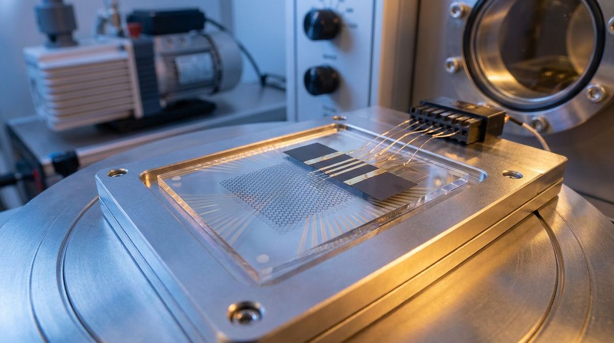
In the development of high-performance graphene electronics, the physical edges of the graphene flake are often the primary bottleneck for carrier mobility. When engineers use standard lithography and plasma etching to define a graphene channel, they create "natural edges." These edges are characterized by disordered carbon atoms and dangling bonds that act as massive scattering centers for electrons. This scattering limits the mean free path of the carriers, effectively capping the performance of the device regardless of how high the intrinsic quality of the graphene is.
For startups and research labs working on ultra-high-speed transistors or precision quantum sensors, this edge scattering is a deal-breaker. If the goal is to reach the theoretical limits of carrier mobility in bilayer graphene, the solution is to avoid physical etching altogether.
The research by Blanda et al. introduces a method to bypass the edge-scattering problem by using electrostatic confinement. Instead of cutting the graphene to create a channel, we use a patterned graphite gate to create a potential barrier that "squeezes" the carriers into a specific path.
By using a graphite-gated architecture, the active device area is completely isolated from the disordered natural edges of the graphene flake. The channel is defined by the electric field of the gate, creating a "soft" boundary. This electrostatic boundary allows the carriers to flow through the center of the flake without ever interacting with the messy, disordered edges. This method has demonstrated quantum mobilities as high as 2.5 x 10^6 cm2/Vs, a value that is significantly higher than what is typically achievable in etched devices.
To attempt this architecture, a lab will require advanced nanofabrication capabilities. This is not a "maker" project for a desktop 3D printer; it requires a cleanroom environment.
1. High-quality Bilayer Graphene (BLG): Ideally exfoliated from high-quality graphite.
2. Hexagonal Boron Nitride (hBN): Used as an ultra-flat encapsulation layer to prevent substrate interference.
3. Graphite Flakes: To be used as the gate material.
4. Electron-Beam Lithography (EBL) System: For high-resolution patterning of the graphite gates.
5. Atomic Force Microscopy (AFM) or Kelvin Probe Force Microscopy (KPFM): To verify surface potential and boundary quality.
6. Cryogenic Probe Station: To measure quantum oscillations (Shubnikov-de Haas effect) at low temperatures.
7. Metal Deposition System (E-beam evaporator): For gold/chromium contact pads.
The following steps outline the process for creating a gate-defined Hall-bar. Note that these steps assume a standard van der Waals heterostructure assembly method.
1. Substrate Preparation: Start with a highly polished SiO2/Si substrate or a thick hBN flake on a substrate to provide a flat foundation.
2. Graphite Gate Patterning: Using EBL, pattern a single layer of graphite onto the substrate or a thin hBN layer. This graphite layer will act as your gate. The pattern should define the shape of your Hall bar (e.g., a long rectangular strip).
3. Bilayer Graphene Placement: Carefully transfer a bilayer graphene flake over the patterned graphite gate. The graphene must overlap the gate area to allow for electrostatic control.
4. Encapsulation: Sandwich the bilayer graphene between two layers of ultra-clean hBN. This is the most critical step. The hBN must be pristine to prevent any charge impurities from entering the channel. The total thickness of the hBN encapsulation is assumed to be between 20nm and 50nm for optimal gate control, though exact dimensions depend on the desired gate capacitance.
5. Contact Formation: Pattern and deposit metal contacts (typically Cr/Au) at the ends of the graphene channel. These contacts must penetrate through the top hBN layer to make direct contact with the graphene.
6. Gate-Defined Channel Activation: Apply a DC voltage to the graphite gate. As the voltage increases, the electrostatic potential will create a channel in the graphene that is defined by the gate geometry rather than the physical edges of the flake.
Once the device is fabricated, the following tests should be performed to validate the high-mobility architecture:
1. Longitudinal and Hall Resistance: Perform standard four-probe measurements. You are looking for a reduction in longitudinal resistance compared to an etched device of the same dimensions.
2. Magnetoresistance Peaks: Apply a perpendicular magnetic field. The research indicates that boundary scattering in these devices shows specific magnetoresistance peaks. If the device is working correctly, these peaks should correlate with the electrostatic boundary defined by the gate.
3. Quantum Oscillation Visibility: This is the ultimate test of mobility. At low temperatures (typically below 4K) and in a magnetic field, look for Shubnikov-de Haas oscillations. The visibility of these oscillations at low magnetic fields (as low as 4 mT) is a direct indicator of the extremely high quantum mobility achieved by avoiding edge scattering.
4. Carrier Density Mapping: Vary the gate voltage to change the carrier density. The research suggests that the effective channel width increases with the Fermi level. You should observe a measurable shift in the transport characteristics as the electrostatic confinement changes.
1. Boundary Disorder: While the electrostatic boundary avoids physical edges, the research notes that the boundary can still be disordered due to the fabrication method. To mitigate this, ensure the graphite gate patterning is extremely clean and that no polymer residue from the lithography process remains on the surface.
2. Gate Leakage: Using graphite as a gate can increase the risk of leakage current if the insulating hBN layer is too thin or has pinholes. We recommend a minimum hBN thickness of 15nm for the gate dielectric layer and should monitor leakage current during the initial voltage sweeps.
3. Contamination: Any organic residue trapped during the hBN encapsulation process will act as a scattering center, negating the benefits of the gate-defined channel. Using a vacuum-based transfer system is highly recommended to maintain the integrity of the heterostructure.
4. Alignment Errors: The success of the device depends on the graphene being perfectly aligned with the graphite gate. Use high-resolution optical microscopy or AFM to verify alignment before proceeding to the encapsulation step.
This guide is based on the findings of Blanda et al. (2026), who demonstrated that a graphite-gated architecture allows for the creation of a fully electrostatically defined Hall-bar. Their work proves that by moving the active transport region away from the natural edges of the graphene, one can achieve a record quantum mobility of 2.5 x 10^6 cm2/Vs. This engineering approach shifts the focus from physical material shaping to electrostatic potential shaping, providing a roadmap for the next generation of high-performance graphene-based quantum electronics.
Serious about B2B integration? Test our premium Pulsed Electrical Resistive Carbon Heating turbostratic graphene in your lab. 100g sample packs available now.
Explore More
Researchers developed coupled dynamical Boltzmann transport equations that include long-range interactions, creating a more accurate model for electron...

Learn how to design and prototype graphene slit junctions for directional electron-beam formation and tunable spin filtering in nanoelectronic devices.

Researchers have developed a hydrodynamic backflow method to ease the fermion sign problem, a major hurdle in quantum simulations of materials like graphene.