
Modeling Electron Transport in 2D Materials with New Boltzmann Equations
Researchers developed coupled dynamical Boltzmann transport equations that include long-range interactions, creating a more accurate model for electron...
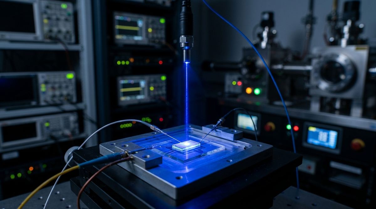
For engineers working in neuromorphic computing, non-volatile memory, or advanced sensing, the combination of two-dimensional materials and ferroelectric oxides offers a powerful solution for high-sensitivity, low-power devices. The core challenge in these hybrid architectures is the coexistence of different charge dynamics. When you apply light to a ferroelectric-graphene device, you are not just changing the resistance; you are interacting with the polarization of the ferroelectric layer itself.
Recent research has demonstrated that the outcome of this interaction depends entirely on the wavelength of light used. This provides a unique engineering opportunity: you can use light to either fine-tune the resistance of a graphene channel (for sensing or weight adjustment in neural networks) or to completely reset the device state (for memory clearing). This guide outlines how to build and test a prototype that utilizes this wavelength-selective control.
The goal is to create a device where the resistance of a graphene channel can be set to a specific value using visible light, or wiped clean using ultraviolet light. This is essentially an optically programmable, non-volatile resistive switch. In a typical memory application, you want to change the state without destroying the underlying polarization. In a reset application, you want to clear the state to return to a baseline.
By selecting the correct photon energy, you can decide whether you are performing a subtle "tuning" operation or a hard "reconfiguration" operation.
To build a laboratory-scale prototype, you will need the following materials. Since exact thicknesses are dependent on your specific deposition equipment, the values provided are cautious engineering assumptions.
Substrate: Silicon with a 285 nm to 300 nm thermal oxide layer (SiO2/Si) is the standard for graphene work.
Graphene: High-quality CVD (Chemical Vapor Deposition) graphene transferred onto the substrate.
Ferroelectric Material: Barium Titanate (BTO) or Lead Zirconate Titanate (PZT) deposited via Atomic Layer Deposition (ALD) or Sputtering. For a prototype, a thickness of 20 nm to 50 nm is recommended.
Electrodes: Gold (Au) or Platinum (Pt) for the top electrode to ensure chemical stability.
Light Sources:
A 365 nm UV LED or laser for the reset/reconfiguration phase.
A 530 nm green LED or laser for the tuning/doping phase.
Measurement Tools:
A high-precision Source Measure Unit (SMU) capable of picoampere resolution.
A probe station for electrical contact.
The assembly of these devices requires careful handling to maintain the integrity of the graphene-ferroelectric interface.
1. Substrate Preparation: Clean the SiO2/Si substrate using a standard RCA cleaning process or a piranha etch to remove organic contaminants.
2. Graphene Deposition: Use a standard PMMA-assisted transfer method to place CVD graphene onto the substrate. Ensure the graphene is continuous and free of excessive polymer residue, as residue will interfere with the ferroelectric interface.
3. Ferroelectric Deposition: Deposit the ferroelectric layer (e.g., BTO) directly onto the graphene. If using ALD, use a low-temperature process (below 250 degrees Celsius) to avoid damaging the graphene or inducing excessive thermal strain. A thickness of 30 nm is a good starting point.
4. Electrode Patterning: Use photolithography to pattern the top electrode. A small circular contact area (e.g., 50 micrometers in diameter) is ideal for localized light interaction.
5. Final Contact: Deposit the gold or platinum layer via thermal evaporation.
The core of this device's utility lies in how you apply light. Based on the physics of photovoltaic screening and defect-mediated excitation, your control logic should follow these two paths:
Strategy A: The Tuning Mode (530 nm)
If your goal is to adjust the resistance of the graphene channel without losing the non-volatile state (the remanent polarization), use 530 nm illumination. At this wavelength, the light primarily induces charge redistribution via defect-state excitation within the ferroelectric. This allows you to tune the carrier concentration in the graphene (doping) while the ferroelectric polarization remains largely intact. This is the mode you would use for "weight updates" in a neuromorphic circuit.
Strategy B: The Reset Mode (365 nm)
If your goal is to clear the memory or reset the device to a baseline state, use 365 nm UV illumination. The higher photon energy induces free carriers that cause photovoltaic charge screening. This screening effectively cancels out the polarization of the ferroelectric layer. According to research, this can cause the resistance ratio between different polarization states to drop significantly (for example, from a high-contrast 290% down to a low-contrast 15%). This is your "factory reset" or "erase" command.
To verify that your prototype is functioning according to these principles, follow this testing sequence:
1. Dark Resistance Baseline: Measure the resistance of the graphene channel in the dark. Apply a voltage pulse to switch the ferroelectric polarization and measure the resistance at both remanent states. You should see a significant difference in resistance (the resistance ratio).
2. Visible Light Tuning Test: Subject the device to 530 nm illumination while measuring the resistance. You should observe a shift in the resistance value, but the ability to switch between high and low resistance states (the resistance ratio) should remain relatively stable.
3. UV Reset Test: Subject the device to 365 nm illumination. Monitor the resistance ratio. You should observe the resistance difference between the two polarization states shrinking drastically, indicating that the polarization has been screened and the device has been "reset."
4. Stability Test: After the UV reset, check if the device can be switched back into a high-contrast state using electrical pulses alone.
The following points represent potential failure modes or assumptions made during this guide:
Interface Quality: The success of this device depends entirely on the quality of the graphene-ferroelectric interface. Any trapped air, moisture, or polymer residue will create parasitic resistance and prevent effective charge transfer.
Dielectric Breakdown: When applying voltages to switch the ferroelectric layer, ensure the voltage does not exceed the dielectric breakdown strength of your specific material (typically 1-5 MV/cm).
Thermal Management: While the light-induced effects are electronic, prolonged exposure to high-intensity lasers can cause local heating, which may also affect the polarization.
Assumed Dimensions: This guide assumes a standard micro-scale device. If you scale up to larger areas, the uniformity of the ferroelectric film becomes much more critical for consistent device performance.
Source Basis: The operational logic and specific resistance ratios (290% to 15%) mentioned in this guide are derived from the research by Maity et al. regarding wavelength-resolved control in photo-ferroelectric/graphene devices.
Serious about B2B integration? Test our premium Pulsed Electrical Resistive Carbon Heating turbostratic graphene in your lab. 100g sample packs available now.
Explore More
Researchers developed coupled dynamical Boltzmann transport equations that include long-range interactions, creating a more accurate model for electron...

Learn how to design and prototype graphene slit junctions for directional electron-beam formation and tunable spin filtering in nanoelectronic devices.

Researchers have developed a hydrodynamic backflow method to ease the fermion sign problem, a major hurdle in quantum simulations of materials like graphene.