
C2DTD: A Physics-Informed Digital Fingerprint to Accelerate Carbon Materials
Researchers developed the CARBON-2D Topological Descriptor (C2DTD), an interpretable, physics-informed method to rapidly predict the properties of new 2D...
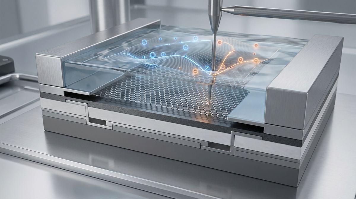
Imagine a world where the limits of computer processing power are no longer dictated by how small we can etch silicon, but by how precisely we can draw with electricity at the atomic level. As our demand for faster, smaller, and more efficient electronics grows, the industry is hitting a wall. Traditional methods of carving patterns into materials are becoming too slow, too expensive, or too destructive to keep up with the needs of next-generation materials like graphene. Researchers are now looking toward a method that behaves more like a microscopic pen, allowing us to write intricate electronic components directly into existence using controlled electrical currents.
For decades, the semiconductor industry has relied on photolithography, a process that uses light to etch patterns onto silicon wafers. While highly successful, this method faces significant physical hurdles as we approach the atomic scale. As features get smaller, the wavelength of the light used becomes a limiting factor, making it difficult to create the ultra-fine structures required for modern high-performance transistors. To go smaller, the industry has turned to electron-beam lithography, which uses a focused beam of electrons to "write" patterns. While incredibly precise, electron-beam lithography is a notoriously slow and expensive process. It requires a vacuum environment and high-energy beams that can inadvertently damage the very materials they are trying to shape.
Graphene presents a unique challenge in this context. Because graphene is a single layer of carbon atoms, its extraordinary electronic properties—such as incredibly high electron mobility—are highly sensitive to the quality of its edges and the integrity of its atomic lattice. If a fabrication process is too harsh, it introduces defects into the hexagonal carbon structure. These defects act as obstacles for electrons, causing scattering that increases resistance and destroys the material's superior performance. Consequently, there has been an urgent need for a nanofabrication method that is both highly precise and "gentle" enough to preserve the pristine nature of the graphene lattice, while also being faster and more direct than current methods.
The breakthrough concept explored by researchers is known as direct-write electrochemical nanofabrication. Instead of using a complex mask or a high-energy electron beam to define a shape, this method uses a controlled electrical current and a liquid medium to "print" features directly onto a surface. Think of it like a high-precision Etch-a-Sketch for the nano-world. By submerging a substrate in an electrolyte and applying a specific voltage through a tiny tip or probe, we can trigger chemical reactions that either deposit material or remove it in very specific locations.
This approach is revolutionary because it bypasses the need for the multi-step, mask-heavy processes used in traditional manufacturing. Because the "writing" is driven by the local electrical field, the resolution is governed by the concentration of the electric field at the point of contact. This allows for the creation of "ultrasmall" devices that are much smaller than what standard optical methods could ever achieve. Essentially, it turns the chemical process of electrolysis into a precision manufacturing tool, allowing scientists to tailor the structure of graphene at a scale that was previously difficult to reach without massive infrastructure.
To understand how this system functions, one must look at the intersection of electrochemistry and solid-state physics. The system typically consists of a graphene-coated substrate placed within an electrolyte solution, which is a liquid containing mobile ions. When an external voltage is applied to a probe or a counter-electrode, it creates an electrochemical potential difference. This potential drives ions in the liquid to move toward or away from the graphene surface.
This movement of ions is the core mechanism. Depending on the polarity of the applied voltage, a redox—or reduction-oxidation—reaction occurs at the interface between the liquid and the graphene. In a reduction-based process, ions in the liquid gain electrons and deposit material onto the graphene, effectively "growing" a component. In an oxidation-based process, the electrical energy breaks the chemical bonds of the material or the carbon lattice itself, removing it from the surface to create a channel or a gap.
The precision of this "direct-write" capability comes from the ability to control the electrical field. By using a very sharp probe, the electric field becomes highly concentrated at the very tip, creating a localized zone of intense electrochemical activity. This allows the researcher to define the edges of a device with nanometer-scale precision. Furthermore, because the energy is delivered via electrochemical potential rather than a high-energy particle beam, the process can be much more controlled. This precision is vital for graphene because it allows for the creation of sharp, clean edges that do not disrupt the seamless sp2 hybridization of the carbon atoms. In graphene, the sp2 hybridization is what creates the famous hexagonal lattice that allows electrons to move with almost no resistance; preserving this structure is the ultimate goal of the fabrication process.
In the study conducted by Xiao Liu and Colm Durkan, the researchers demonstrated the ability to use this electrochemical approach to fabricate ultrasmall graphene devices. The significance of their findings lies in the scale and the structural integrity of the resulting devices. By utilizing direct-write electrochemical techniques, they were able to define features that fall into the "ultrasmall" category, which is critical for the next generation of nano-electronics.
The results indicated that the electrochemical method could successfully create the intricate geometries required for functional electronic components, such as junctions or channels, without the massive overhead of traditional lithography. This suggests that the method is not just a theoretical curiosity but a viable path toward creating highly precise, small-scale graphene structures. The ability to control the process at such a minute level means that the researchers could potentially manipulate the electronic properties of the graphene by precisely defining its boundaries, a feat that is essential for creating advanced quantum or high-frequency devices.
The implications of being able to fabricate ultrasmall graphene devices are profound for the future of technology. As devices shrink, the "mean free path" of an electron—the distance an electron travels before hitting something—becomes a critical metric. In graphene, this distance is exceptionally large. If we can manufacture devices that are small enough and have edges clean enough, we can achieve "ballistic transport," where electrons move through the material with almost no resistance. This would lead to transistors that switch at much higher frequencies and consume significantly less power.
Furthermore, the ability to write directly onto the material solves the scalability bottleneck. While current high-end fabrication is limited by the complexity of masks and vacuum chambers, a direct-write electrochemical method offers a path toward more streamlined production. If the process can be refined, it could allow for the rapid prototyping of new electronic architectures. Instead of spending weeks designing and executing a complex lithography run, engineers could potentially "draw" a new circuit design directly onto a substrate, drastically accelerating the pace of innovation in semiconductor research.
While this research marks a significant step forward, it is important to distinguish these laboratory successes from commercially ready technology. One of the primary limitations of electrochemical nanofabrication is the environment itself. Because the process occurs in a liquid electrolyte, transferring the finished device from the liquid into a dry, functional environment without damaging it is a major engineering challenge. Any residue from the electrolyte or the chemical reactions could contaminate the device and alter its electrical properties.
Additionally, there is the question of scalability and uniformity. While it is possible to write a single, perfect device using a microscopic probe, doing so across an entire silicon wafer containing billions of transistors is a much more difficult task. Maintaining a consistent electrochemical environment and ensuring that the "writing" is uniform across large areas requires extreme precision in fluid dynamics and electrical control. Future research will need to focus on how to transition this from a single-device laboratory technique to a high-throughput industrial process that can maintain the same level of atomic precision across large-scale manufacturing lines.
The ability to create ultrasmall, high-integrity graphene devices opens the door to several transformative technologies. One of the most exciting is in the realm of quantum computing. Many quantum architectures require the ability to define extremely small, localized potentials to trap single electrons or manipulate quantum states. Graphene’s unique properties, combined with precise electrochemical patterning, could provide the platform needed for more stable and scalable quantum bits (qubits).
In the world of consumer electronics, this could translate to high-frequency transistors capable of operating in the terahertz range, enabling ultra-fast communication networks like the next evolution of 6G or beyond. Additionally, graphene-based sensors created through this method could be used in medical diagnostics or environmental monitoring. Because the device is so small and the surface area is so precisely controlled, the sensitivity to minute chemical or physical changes is massively increased, allowing for the detection of single molecules or single-atom displacements.
If you remember only one thing from this research, let it be that the way we build the future of electronics is shifting from "carving with light" to "writing with electricity," allowing us to unlock the full, untapped potential of materials like graphene by creating them with unprecedented atomic precision.
What is graphene and why is it special?
Graphene is a single layer of carbon atoms arranged in a hexagonal lattice. It is incredibly thin, yet it is one of the strongest materials known and possesses extraordinary electrical conductivity. Its electrons move through the lattice much faster than they do in silicon, which makes it a prime candidate for much faster computer chips.
Why is traditional lithography not enough for graphene?
Traditional photolithography uses light to create patterns, but light has a wavelength limit that makes it difficult to create extremely small features. Other methods, like electron-beam lithography, are precise but are often too slow for mass production and can damage the delicate carbon structure of graphene, reducing its performance.
How does the electrochemical method work?
The electrochemical method uses a liquid electrolyte and a controlled electric current to shape the material. By applying a specific voltage, you can trigger chemical reactions that either add material to or remove material from the surface. This allows for highly precise, direct-writing of patterns at a very small scale.
What does "direct-write" mean in this context?
Direct-write refers to a manufacturing process where you create a pattern directly on the target material without needing a physical template or a mask. It is similar to how a printer works, where the print head moves across the paper to create the image, rather than using a stencil.
Is this technology ready for my smartphone?
Not yet. While the research shows that we can successfully create tiny, high-performance graphene devices in a laboratory setting, there are still significant engineering hurdles to overcome. We need to find ways to scale this process up for mass production and ensure that the devices can be handled and packaged without losing their performance.
The research by Xiao Liu and Colm Durkan represents a vital step toward a new era of nanofabrication. By moving away from the blunt tools of traditional lithography and toward the precision of electrochemical direct-writing, scientists are gaining the ability to shape the future of electronics at the atomic scale. While challenges in scalability and environmental control remain, the ability to fabricate ultrasmall graphene devices with high structural integrity provides a clear roadmap for the next generation of high-speed, low-power, and quantum-ready electronic technologies.
Serious about B2B integration? Test our premium Pulsed Electrical Resistive Carbon Heating turbostratic graphene in your lab. 100g sample packs available now.
Explore More
Researchers developed the CARBON-2D Topological Descriptor (C2DTD), an interpretable, physics-informed method to rapidly predict the properties of new 2D...

Learn how to create p-n junctions in graphene by selectively oxidizing the underlying germanium substrate. This guide covers a practical method for...

Explore a breakthrough graphene-silicon slot-waveguide modulator. This high-speed device operates at both 1.5 μm and 2 μm, promising next-gen optical networks.