
Hydrodynamic Backflow for Easing the Fermion Sign in Finite-Temperature Electron
Researchers have developed a hydrodynamic backflow method to ease the fermion sign problem, a major hurdle in quantum simulations of materials like graphene.
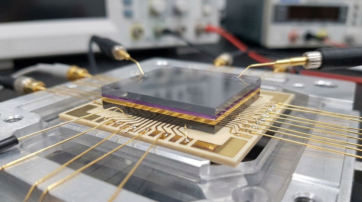
The transition from charge-based electronics to spintronics is driven by the need for lower power consumption and higher processing speeds. In traditional electronics, information is carried by the movement of electrons (charge). In spintronics, information is carried by the electron spin. One of the most difficult engineering hurdles in spintronics is the efficient conversion between charge currents and spin currents.
Recent research has identified a specific material architecture that solves this: WSe2-intercalated bilayer graphene. By sandwiching a monolayer of Tungsten Diselenide (WSe2) between two layers of graphene, we create a system where the wavefunction of the electrons is delocalized across both layers. This creates a unique phenomenon known as the nonlocal Rashba-Edelstein effect. In a device built with this material, a charge current injected into the top graphene layer generates a spin accumulation in the bottom graphene layer. This allows for a nonlocal spin-to-charge conversion that is robust and, crucially, switchable.
This guide outlines how to prototype a four-electrode device capable of demonstrating this effect, providing a foundation for next-generation spintronic logic gates.
The goal is to construct a four-terminal heterostructure device. The device must allow for independent electrical access to the top and bottom graphene layers. The primary functional objective is to demonstrate two things:
1. Nonlocal Spin Accumulation: Injecting a charge current through the top layer (Source 1 and Drain 1) produces a measurable voltage in the bottom layer (Source 2 and Drain 2) due to the spin-to-charge conversion.
2. Layer-Selective Chirality Switching: By switching the current injection from the top layer to the bottom layer, the sign of the induced spin accumulation in the opposite layer should flip. This provides a mechanical/electrical way to switch the logic state (0 or 1) without moving parts.
To achieve the precision required for these quantum effects, the following materials are necessary. Note that because the research is based on high-quality van der Waals heterostructures, standard industrial CVD (Chemical Vapor Deposition) may lack the required crystal quality; mechanical exfoliation and dry-transfer methods are recommended for lab-scale prototyping.
1. Bilayer Graphene (BLG): High-mobility graphene flakes, preferably exfoliated from graphite.
2. WSe2 Monolayer: A high-quality monolayer of Tungsten Diselenide to act as the intercalant.
3. Substrate: Hexagonal Boron Nitride (hBN) on a Silicon/Silicon Dioxide (Si/SiO2) base. hBN is essential to minimize substrate interference and maintain high carrier mobility.
4. Contact Metal: Gold (Au) for the top layer and a combination of Titanium (Ti) and Gold (Au) for the bottom layer to ensure low contact resistance.
5. Lithography Equipment: Electron-beam lithography (EBL) system for defining sub-micron electrode patterns.
6. Deposition System: Thermal evaporator or electron-beam evaporator for metal deposition.
The following steps assume a standard "dry transfer" or "pick-up" method using a polymer stamp (such as PC or PDMS).
1. Substrate Preparation: Clean an hBN-on-SiO2 substrate using plasma cleaning to remove organic residues.
2. Bottom Layer Deposition: Exfoliate a high-quality monolayer of graphene and transfer it onto the hBN substrate.
3. Intercalation Layer: Transfer a monolayer of WSe2 onto the first graphene layer. It is critical that the WSe2 layer is continuous and free of wrinkles, as wrinkles can disrupt the wavefunction overlap required for the Rashba-Edelstein effect.
4. Top Layer Deposition: Transfer a second layer of graphene onto the WSe2 layer. This creates the WSe2-intercalated bilayer graphene structure.
5. Electrode Patterning (Bottom Layer): Use EBL to define four contact pads on the bottom layer. This requires etching through the top graphene layer or using a very thin top layer that can be selectively contacted. For a simplified prototype, focus on creating contacts that penetrate the top layer or use a thin-film approach.
6. Electrode Patterning (Top Layer): Repeat the EBL process to define two additional contact pads on the top graphene layer.
7. Metallization: Deposit the Ti/Au contacts. For the bottom layer, the metal must make direct contact with the graphene through the top layer or via a carefully controlled etching process.
8. Annealing: Perform a vacuum anneal at approximately 200 to 300 degrees Celsius to improve contact resistance and remove any polymer residue from the transfer process.
Once the device is fabricated, the following testing sequence should be used to verify the Rashba-Edelstein effect.
1. Device Geometry Verification: Use Atomic Force Microscopy (AFM) to confirm the thickness of the layers and the presence of the WSe2 monolayer.
2. Basic Transport Characterization: Perform standard four-probe resistance measurements to ensure the graphene layers are conductive and the contact resistance is within acceptable limits (typically < 1 kOhm for research-grade devices).
3. Nonlocal Voltage Measurement:
- Apply a constant current (I1) through the top layer electrodes (Source 1 and Drain 1).
- Measure the voltage (V2) across the bottom layer electrodes (Source 2 and Drain 2) using a high-impedance lock-in amplifier.
- A non-zero voltage in the bottom layer, despite no direct current flow through it, confirms the nonlocal Rashba-Edelstein effect.
4. Chirality Switching Test:
- Repeat the measurement, but inject the current (I1) through the bottom layer electrodes.
- Observe the polarity of the voltage (V2) in the top layer. According to the research, the sign of the voltage should flip, demonstrating the chirality switch.
Because this is a research-based prototype, several parameters must be assumed for the initial build.
1. Channel Dimensions: The research does not specify exact device geometry. For a lab prototype, assume a channel length of 10 micrometers and a contact width of 100 nanometers. Smaller dimensions will increase the signal-to-noise ratio but increase fabrication difficulty.
2. Operating Temperature: While the research suggests the effect is robust to temperature, initial testing should be conducted at cryogenic temperatures (4K to 77K) to clearly distinguish the spin-induced signal from thermal noise. Once the signal is confirmed, testing should proceed at room temperature.
3. Twist Angle: The research states the effect is robust to twist angle modulation. However, for the first prototype, assume a near-zero twist angle (aligned layers) to maximize the hybridization of the wavefunctions.
4. Electric Field: The effect is robust to moderate vertical electric fields. In a real device, an external gate voltage (using the Si/SiO2 substrate as a back-gate) should be used to tune the Fermi level into the regime where the Rashba-Edelstein effect is most prominent.
1. Layer Delamination: The most significant risk is the mechanical failure of the heterostructure during the transfer of the second graphene layer.
- Mitigation: Use the "pick-up" method with a polymer stamp to ensure the layers are pressed together with uniform pressure, minimizing trapped air or moisture.
2. Contact Resistance: High contact resistance at the bottom layer can drown out the nonlocal voltage signal.
- Mitigation: Use electron-beam lithography for extremely precise contact placement and perform a controlled vacuum anneal to ensure metal-to-graphene contact.
3. Signal-to-Noise Ratio: The nonlocal voltage generated by the Rashba-Edelstein effect is extremely small.
- Mitigation: Use a Lock-in amplifier with a low-frequency AC current source to filter out thermal and electromagnetic noise.
4. Material Contamination: Any residue from the transfer polymer (PC/PDMS) will act as a scattering center, destroying the spin-to-charge conversion.
- Mitigation: Implement rigorous cleaning protocols, including high-temperature vacuum annealing and potentially oxygen plasma cleaning (used with extreme caution to avoid damaging the graphene).
This guide is based on the research findings of Milivojević, Mnich, and Gmitra (2026) regarding WSe2-intercalated bilayer graphene. The core physical principles—the nonlocal Rashba-Edelstein effect and the layer-selective chirality switch—are derived directly from their theoretical and computational models. The engineering steps and material choices are practical extrapolations intended to translate these quantum mechanical observations into a physical laboratory prototype.
Serious about B2B integration? Test our premium Pulsed Electrical Resistive Carbon Heating turbostratic graphene in your lab. 100g sample packs available now.
Explore More
Researchers have developed a hydrodynamic backflow method to ease the fermion sign problem, a major hurdle in quantum simulations of materials like graphene.

Learn to build a prototype active graphene metasurface for mid-IR beam steering. This guide covers the materials, fabrication, and testing for LiDAR.

Researchers use the Generalized Beth-Uhlenbeck approach to model electron interactions in 2D materials, offering a new way to predict graphene's behavior.