
An Exact Solution for Electron Transport and Resistivity in the Hubbard Model
Researchers derived the first exact formula for resistivity in the 1D infinite-U Hubbard model, providing a crucial benchmark for understanding strongly...
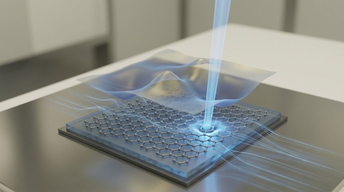
Imagine a material so thin that it consists of only a single layer of atoms, yet it possesses the ability to move electricity with almost zero resistance. This is graphene, a substance that has promised to revolutionize everything from the smartphone in your pocket to the massive data centers that power the internet. However, graphene is not a static material; it is a sensitive one. When we hit it with high-energy particles, its fundamental behavior changes in ways that are incredibly difficult to track because these changes happen in a fraction of a trillionth of a second. To master graphene, we cannot just look at how it works when it is perfect; we must understand exactly what happens when it is disrupted. This is the frontier of research conducted by Yifan Yao and Andre Schleife, who have investigated the ultrafast electron dynamics of graphene when it is subjected to electron irradiation. Their work seeks to understand the chaotic, lightning-fast dance of electrons as they navigate the structural changes caused by high-energy bombardment.
For decades, the semiconductor industry has relied on silicon to drive the digital age. Silicon has served us well, but it is approaching a physical wall. As we try to make transistors smaller and faster, silicon generates more heat and encounters more resistance, limiting its potential for future speed increases. Graphene has been proposed as the successor because its electrons move at incredibly high velocities. However, there is a massive engineering hurdle: graphene is highly sensitive to its environment and its own structural integrity.
If we want to use graphene in real-world high-speed circuits, we need to know how it behaves when it is not perfect. In manufacturing, it is nearly impossible to create a perfectly flawless sheet of graphene. Furthermore, sometimes we want to intentionally create defects to tune the material's properties—a process known as defect engineering. The problem is that we currently lack a complete, high-resolution understanding of how these defects influence the speed at which electrons move and how they lose their energy. Without knowing the precise timescales of how electrons react to being struck by an electron beam, engineers cannot accurately predict how a graphene-based chip will perform under high-frequency operation. We are essentially trying to design a high-speed racing engine without knowing exactly how the fuel behaves when the engine gets hot or the fuel lines are slightly dented.
To understand this research, imagine a perfectly smooth, frozen lake. A group of ice skaters is gliding across it at incredible speeds. In this analogy, the ice skaters represent the electrons, and the smooth surface of the lake represents a pristine, flawless sheet of graphene. Because the ice is smooth, the skaters can glide almost indefinitely without losing momentum.
Now, imagine that someone begins firing small, high-velocity pebbles onto the ice. These pebbles don't just sit on the surface; they create small cracks and pits in the ice. These cracks and pits are the defects caused by electron irradiation. As the skaters encounter these cracks, they have to change direction, they might stumble, or they might lose speed as they hit the uneven terrain. The research by Yao and Schleife is essentially a high-speed camera study of these skaters. They aren't just looking at whether the skaters slow down; they are looking at exactly how many picoseconds it takes for a skater to react to a crack, how much energy they lose when they hit it, and how the presence of many cracks changes the overall flow of skaters across the lake. By understanding these tiny, fast interactions, we can learn how to design better tracks or even place the cracks in specific patterns to guide the skaters more efficiently.
To understand the physics, we must first look at the structure of graphene. Graphene is a two-dimensional lattice of carbon atoms arranged in a hexagonal pattern. Each carbon atom is bonded to its neighbors through strong covalent bonds, creating a highly stable and conductive structure. The electrons in graphene are not stuck to a single atom; instead, they exist in a massive, shared cloud known as the pi-electron system. This allows them to move through the lattice with extraordinary mobility.
Electron irradiation is a process where a beam of high-energy electrons is directed at the graphene sheet. When a high-energy electron from the beam hits a carbon atom in the lattice, it can transfer enough kinetic energy to knock that carbon atom out of its position. This creates a vacancy, which is a hole where an atom used to be. This vacancy is a major structural defect. It breaks the perfect symmetry of the hexagonal lattice and leaves behind dangling bonds—unpaired electrons that are looking for something to connect to.
These defects change the electronic landscape of the graphene. In a perfect sheet, electrons move according to a unique relationship between their energy and their momentum, known as the Dirac cone. This relationship is what makes graphene so fast. However, when a vacancy is created, it acts as a scattering center. A scattering center is an obstacle that interrupts the path of an electron. When an electron hits a defect, it undergoes a scattering event, which changes its momentum and its energy. This process is called electron-phonon coupling. The energy that the electron loses during this collision is transferred to the lattice itself, causing the carbon atoms to vibrate. These vibrations are called phonons. The interaction between the moving electrons and these lattice vibrations is the core of electron dynamics.
The research conducted by Yifan Yao and Andre Schleife focuses on the timescales of these interactions. When graphene is irradiated, the researchers observed how the energy of the excited electrons is redistributed throughout the material. They found that the presence of irradiation-induced defects fundamentally alters the relaxation pathways of the electrons. In pristine graphene, an excited electron might stay in its high-energy state for a relatively long time before it loses that energy to the lattice.
However, once the electron beam has created defects, the "rules" of the game change. The defects introduce new available states for the electrons to scatter into. This means that instead of having only a few ways to lose energy, the electrons now have many more "exit ramps." This leads to much faster energy relaxation. The researchers discovered that the dynamics are incredibly sensitive to the density of these defects. As the dose of electron irradiation increases, the time it takes for the electrons to return to their ground state decreases significantly.
Furthermore, the study highlights that the defects do not just slow the electrons down; they change how the energy is distributed across the lattice. The interaction between the electrons and the phonons becomes much more complex. The researchers were able to observe that the irradiation creates a localized change in the electronic density of states, meaning the material's ability to conduct electricity is no longer uniform across the sheet. The energy is not just being lost; it is being redistributed in a way that is dictated by the specific pattern and density of the holes left behind by the electron beam.
This research is vital because it provides a roadmap for what scientists call defect engineering. For a long time, the goal in materials science was to create perfect materials. But as we move into the era of nano-electronics, we are realizing that perfection is not always the goal. We want materials that we can tune. If we can precisely control how many defects are created and where they are located, we can create graphene with specific electrical properties that do not exist in nature.
For example, we could create a graphene material that has a specific energy bandgap, which is something pristine graphene lacks. This would allow graphene to be used in more traditional transistor applications where being able to turn the current "off" is just as important as being able to turn it "on." By understanding the ultrafast dynamics, engineers can predict how much heat will be generated when an electron hits a defect. This is crucial for thermal management in microchips. If we know how quickly energy is transferred from electrons to phonons, we can design better cooling systems or structure the material to dissipate heat more effectively. This research moves us from a period of accidental discovery to a period of intentional, precision design at the atomic level.
While these findings are groundbreaking, it is important to recognize that this research is fundamental and theoretical in nature. The study focuses on the fundamental physics of how electrons and defects interact, which is a necessary step before any commercial application can be realized. There are several significant hurdles that still need to be overcome.
First, there is the challenge of scalability. While an electron beam can create very precise defects in a laboratory setting, using such a method to modify large, continuous sheets of graphene for mass production is a massive engineering challenge. Second, there is the issue of stability. A defect created by an electron beam is a point of weakness in the material. We need to ensure that these defects do not lead to the gradual degradation of the material over time when it is used in a device. Finally, the spatial resolution required to place defects with the precision needed for advanced logic circuits is incredibly high. We need to know if we can control these "pebbles on the ice" with enough accuracy to build complex, functioning circuits.
Despite the challenges, the potential applications are vast. In the realm of high-frequency communications, graphene-based devices could enable signals to be processed at much higher frequencies than current silicon technology allows. This would be essential for the next generation of 6G and beyond wireless networks.
In the field of sensing, the extreme sensitivity of graphene's electronic state to its structural integrity means that even a single defect can cause a measurable change. This could lead to the development of ultra-sensitive sensors capable of detecting single molecules or tiny changes in environmental conditions, which has massive implications for medical diagnostics and environmental monitoring.
Furthermore, in the field of quantum computing, the ability to precisely control defects and electronic states is critical. Defects in graphene can sometimes act as sites for quantum bits, or qubits. If we can master the dynamics of these defects, we might be able to create more stable and controllable quantum systems. Finally, ultrafast photodetectors, which convert light into electrical signals at incredibly high speeds, could benefit immensely from the knowledge of how electrons relax after being excited by light.
If you remember only one thing from this research, let it be this: the ability to control the "imperfections" in graphene through electron irradiation is the key to unlocking its true potential as a tunable, high-performance material for the next generation of electronics.
What is graphene and why is it special?
Graphene is a single layer of carbon atoms arranged in a hexagonal lattice. It is special because it is incredibly thin, extremely strong, and allows electrons to move through it at very high speeds with very little resistance, which makes it a candidate for ultra-fast electronics.
How does electron irradiation affect graphene?
Electron irradiation involves hitting graphene with a beam of high-energy electrons. This can knock carbon atoms out of their positions in the lattice, creating holes or vacancies. These vacancies act as obstacles that change how electricity flows through the material.
Why is the speed of electron movement so important?
In modern computing, the speed at which electrons can move and relax after being excited determines how fast a processor can operate. If we want faster computers and communications, we need materials where these electron movements are extremely rapid and predictable.
What is defect engineering?
Defect engineering is the practice of intentionally introducing specific flaws or irregularities into a material to change its properties. Instead of trying to make a material perfect, scientists use defects to "tune" the material for specific tasks, like creating a certain electrical conductivity or a specific chemical sensitivity.
Can we use this research to make better smartphones?
While this research is currently focused on the fundamental physics of materials, the knowledge it provides is essential for developing the next generation of semiconductor materials. Once we can control these electron dynamics and defects at scale, it could lead to much faster and more efficient electronic components in devices like smartphones.
The study of ultrafast electron dynamics in electron-irradiated graphene, as explored by Yifan Yao and Andre Schleife, represents a critical step in the evolution of nanotechnology. By moving beyond the study of perfect crystals and diving into the complex, fast-paced world of defect-driven dynamics, we are gaining the tools necessary to engineer the materials of the future. While the path from fundamental physics to a consumer-ready graphene chip is long and filled with engineering challenges, understanding the way electrons dance around atomic-scale obstacles is the first step toward a new era of electronic innovation.
Serious about B2B integration? Test our premium Pulsed Electrical Resistive Carbon Heating turbostratic graphene in your lab. 100g sample packs available now.
Explore More
Researchers derived the first exact formula for resistivity in the 1D infinite-U Hubbard model, providing a crucial benchmark for understanding strongly...

Learn how to utilize bipartite-lattice symmetry to generate pure spin shift currents in graphene nanoribbons for advanced spintronic device prototyping.

Researchers propose a novel method to detect spin- and valley-polarized states in van der Waals materials, a key step for next-gen spintronics and...