
Unlocking Superconductivity in Twisted Graphene: A Gutzwiller Study Explained
Explore how theoretical physics unlocks the secrets of strongly correlated superconductivity in twisted bilayer graphene, a key step toward future quantum...
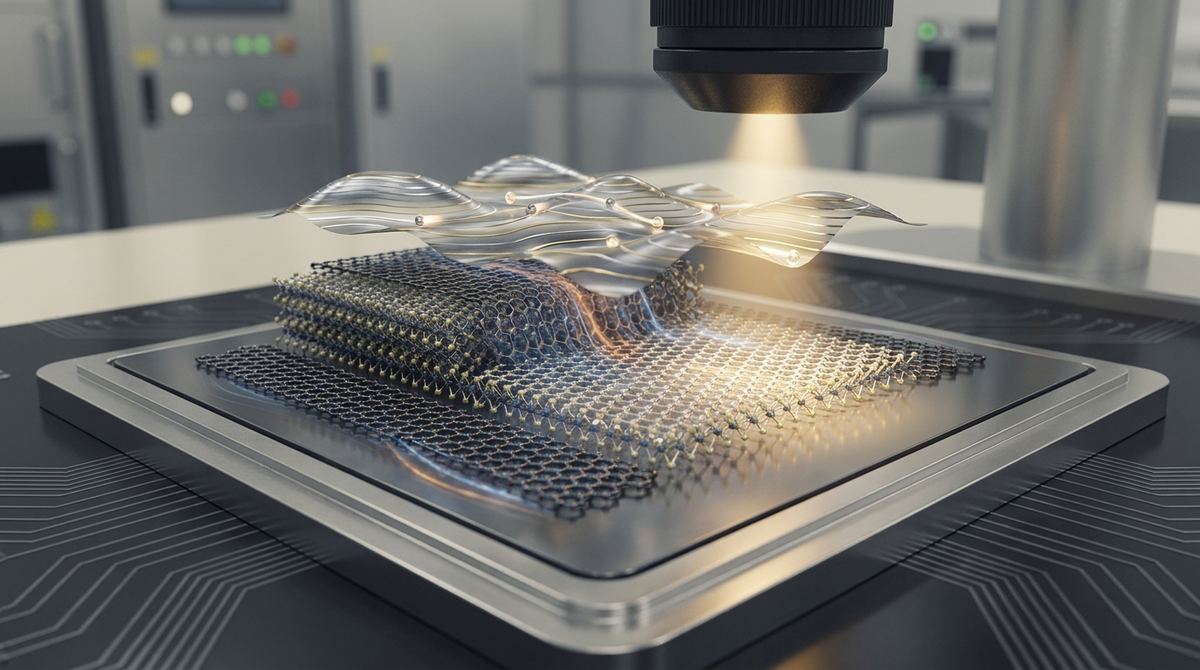
Imagine a material that changes its fundamental identity simply because you changed its thickness. If you have a stack of many layers, the material might be useful for one specific electronic task, but if you peel it down to a single layer of atoms, its very ability to interact with light changes entirely. This is not science fiction; it is the reality of the world of two-dimensional materials. In recent work, researchers Maciej Bazarnik, Thorsten Deilmann, Marta Przychodnia, and Anika Schlenhoff have explored how the thickness of molybdenum disulfide, known as MoS2, determines its electronic band gap. This discovery is critical because it provides a roadmap for how engineers can design the next generation of transistors and light-emitting devices by precisely controlling the number of atomic layers present in a device.
For decades, the semiconductor industry has relied on silicon to power everything from smartphones to supercomputers. However, silicon is a bulk material with a fixed electronic band gap. This means its ability to conduct electricity or interact with light is set in stone by its crystal structure. As we attempt to make transistors smaller and smaller to increase computing power, silicon faces significant physical hurdles. When devices reach the atomic scale, silicon suffers from increased electrical leakage and thermal issues that can lead to device failure.
Furthermore, silicon is an indirect band gap material. In the realm of physics, this means it is quite poor at interacting with light. If you want to build a highly efficient light-emitting diode (LED) or a sensitive photodetector, silicon is fundamentally limited by its electronic structure. To move beyond the limitations of silicon, we need materials that offer more versatility. We need materials where the electronic properties can be "tuned" or adjusted. The challenge for researchers has been finding a way to grow these two-dimensional materials with such extreme precision that we can use thickness as a control knob to dictate how the material behaves.
To understand this research, we must first understand the concept of a band gap. In any solid material, electrons exist in specific energy levels. The band gap is the "forbidden" energy zone between the level where electrons are normally seated and the level where they can move freely to conduct electricity. If the gap is large, the material is an insulator; if the gap is small, it is a semiconductor.
The key idea in this research is that the size and nature of this gap are not fixed for molybdenum disulfide. When the material is in its bulk form—meaning it has many, many layers stacked together—it has an indirect band gap. In an indirect band gap, an electron needs a little extra help (a boost of momentum from a vibration in the crystal) to jump across the gap. This makes it inefficient for light-based applications. However, when you thin the material down to a single monolayer, the electronic structure shifts, creating a direct band gap. In a direct band gap, the electron can jump the gap simply by absorbing a photon, making the material incredibly efficient at interacting with light. This transition from indirect to direct is the "holy grail" for creating ultra-thin, light-sensitive electronics.
While molybdenum disulfide is a different chemical compound, it belongs to the same family of two-dimensional materials as graphene. These materials are characterized by strong internal bonds within the layer, but very weak bonds between the layers, allowing them to be exfoliated or grown in thin sheets. To study these effects with scientific rigor, the researchers used a technique called Molecular Beam Epitaxy, or MBE.
MBE is one of the most precise manufacturing methods in existence. It takes place inside an ultra-high vacuum chamber, which is necessary to prevent any stray air molecules from contaminating the growing crystal. Inside this vacuum, elemental sources of molybdenum and sulfur are heated in specialized containers called Knudsen cells. These elements evaporate and travel in straight, parallel "beams" toward a substrate, which is the base upon which the material is built.
By controlling the rate at which these beams hit the substrate, the researchers can add one atomic layer at a time. This is essentially 3D printing at the atomic scale. As each new layer of MoS2 is deposited, the electronic coupling between the layers changes. In a thick stack, the layers interact heavily, influencing the energy levels of the electrons and maintaining that indirect band gap. As the layers are removed or not added, the quantum confinement effect begins to dominate. Quantum confinement occurs because the electrons are restricted to a much smaller space, which forces their energy levels to shift, eventually leading to the direct band gap seen in the monolayer.
The study by Bazarnik, Deilmann, Przychodnia, and Schlenhoff provides a detailed look at how the band gap evolves as the thickness of the MoS2 changes. Using the high-precision environment of MBE, they were able to observe the specific energy transitions that occur as the material moves from a thick, multi-layer state to a thin, few-layer state.
The researchers confirmed that the band gap is highly sensitive to the number of layers. They observed that as the number of layers increases, the energy required to excite an electron changes in a predictable, mathematical way. This is due to the increasing interlayer coupling; as more layers are added, the electronic wavefunctions of the electrons overlap more significantly with the layers above and below, shifting the energy of the conduction and valence bands.
Crucially, the research highlights the ability of MBE to produce high-quality, consistent films. One of the biggest hurdles in studying these properties is that defects in the crystal lattice can "smear" the band gap, making it difficult to see the clear transition from indirect to direct. The precision of the MBE method allows for a cleaner observation of these quantum mechanical effects, providing a clear dataset that shows exactly how the electronic properties shift as the material reaches its monolayer limit.
The implications of this research are vast, particularly for the field of optoelectronics. Because we now have a better understanding of how thickness controls the band gap, engineers can design devices with specific optical properties by simply deciding how many layers of MoS2 to deposit.
For example, if a company wants to create a new type of infrared sensor, they might choose a specific number of layers that provides a band gap tuned exactly to the wavelength of infrared light. If they want to create a high-speed transistor for high-frequency communication, they might aim for a monolayer to take advantage of the direct band gap and high carrier mobility.
This research bridges the gap between theoretical physics and practical engineering. It moves us away from the "one size fits all" approach of silicon and toward a future where material properties are engineered layer by layer. This precision is essential for the development of integrated photonics, where light and electricity are manipulated on the same chip, potentially leading to much faster data processing and communication speeds.
While these findings are significant, it is important to note that this research is currently at a fundamental level. The use of Molecular Beam Epitaxy, while extremely precise, is a slow and expensive process. Currently, it is difficult to scale MBE growth to the large-scale wafers required for mass-market semiconductor manufacturing. While we can grow a perfect monolayer on a small research sample, doing so across a twelve-inch silicon wafer is a massive engineering challenge.
Furthermore, the interaction between the MoS2 and the substrate it is grown on can influence the results. In a laboratory setting, researchers often use specialized substrates to ensure the best crystal quality, but in a real-world device, the material might be placed on different surfaces that could shift the band gap or introduce defects. Future research must focus on how these materials behave when integrated into complex, multi-material device architectures and whether the precision seen in the lab can be maintained in a commercial manufacturing environment.
The ability to tune the band gap of MoS2 opens the door to several transformative technologies. First, we will likely see a revolution in flexible electronics. Because these 2D materials are incredibly thin and strong, they can be integrated into flexible, transparent displays or wearable sensors that conform to the human body.
Second, the direct band gap of the monolayer makes it ideal for next-generation LEDs and micro-LEDs. These could be used in ultra-high-definition displays that are much more energy-efficient than current technologies. Third, in the field of sensing, MoS2 can be used to create sensors that are sensitive to a single molecule of a specific gas. The high surface-to-volume ratio of a monolayer means that every single atom is "exposed" to the environment, making the electrical signal extremely sensitive to even the smallest chemical change.
If you take away only one concept from this research, let it be this: in the world of two-dimensional materials, thickness is destiny. By controlling the number of atomic layers in a material like MoS2, we can fundamentally change how it interacts with light and electricity, turning a bulk semiconductor into a highly efficient light-emitter.
What is the difference between an indirect and a direct band gap?
A direct band gap occurs when the highest energy level of the valence band and the lowest energy level of the conduction band align at the same momentum. This allows electrons to transition between them by absorbing a photon alone. An indirect band gap requires the electron to also change its momentum, usually by interacting with a lattice vibration called a phonon, which makes the process much less efficient for light emission.
Why is molybdenum disulfide (MoS2) important?
MoS2 is a transition metal dichalcogenide that belongs to the class of 2D materials. It is highly valued because it undergoes a dramatic transition from an indirect band gap in its bulk form to a direct band gap in its monolayer form, making it extremely versatile for both electronic and optical applications.
What is Molecular Beam Epitaxy (MBE)?
Molecular Beam Epitaxy is an advanced method of material growth used in ultra-high vacuum environments. It involves creating controlled beams of atoms that are deposited onto a substrate layer by layer. This allows scientists to build materials with atomic-scale precision, which is necessary for studying the properties of 2D materials.
How does thickness affect the properties of a 2D material?
The thickness of a 2D material determines the degree of quantum confinement and the level of interlayer coupling. As a material becomes thinner, the electrons are restricted to a smaller volume, which shifts their energy levels. This change in electronic structure can transform the material's band gap from indirect to direct.
Is this technology ready for my smartphone?
Not yet. While the science is well-understood and being demonstrated in highly controlled laboratory settings, the manufacturing processes like MBE are currently too slow and expensive for mass production. Significant engineering work is needed to scale these processes for commercial electronics.
The research conducted by Maciej Bazarnik, Thorsten Deilmann, Marta Przychodnia, and Anika Schlenhoff represents a vital step in our mastery of the atomic scale. By demonstrating how the band gap of MoS2 responds to thickness variations, they have provided the foundational knowledge required to engineer materials for the next generation of technology. As we move toward a future of flexible, ultra-fast, and light-based electronics, the ability to control matter one layer at a time will be the cornerstone of modern innovation.
Serious about B2B integration? Test our premium Pulsed Electrical Resistive Carbon Heating turbostratic graphene in your lab. 100g sample packs available now.
Explore More
Explore how theoretical physics unlocks the secrets of strongly correlated superconductivity in twisted bilayer graphene, a key step toward future quantum...

Explore how the intrinsic band geometry of 2D materials can induce valley polarization of chiral excitons, a key step toward next-gen valleytronics.

Explore a new class of pressure sensors using graphene to detect pressure-enhanced polarization in ferroelectric boron nitride, a novel slidetronic effect.