
Interaction-driven transport in a non-degenerate mixture of Dirac and massive
Researchers explore interaction-driven transport in graphene, where massless Dirac fermions can drag massive particles, creating a current without direct...
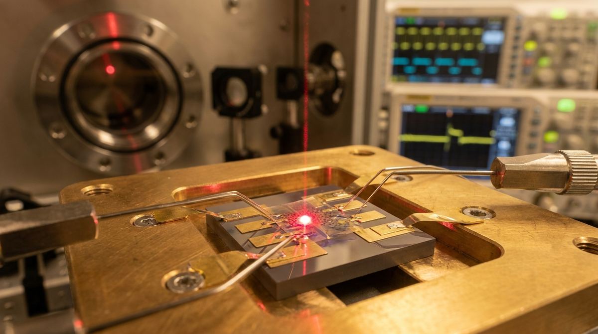
Graphene is a superstar in the world of optoelectronics due to its incredible carrier mobility and broad-spectrum absorption. However, engineers face a persistent hurdle when using graphene for high-speed optical sensing: the persistence effect. Most graphene-based photodetectors rely on a mechanism called trap-mediated photogating. While this mechanism allows for massive sensitivity (high gain), it works by trapping charge carriers in material defects or interfaces. These trapped charges take a long time to release, causing a slow "tail" in the electrical signal. For an engineer trying to detect rapid, repetitive optical pulses—such as those used in high-speed telecommunications or precision photon counting—this persistence is a dealbreaker. It blurs the signal and prevents high-frequency operation.
The research published by Kaur Gill et al. (2026) provides a solution to this specific bottleneck. By integrating a ferroelectric material—specifically rhombohedrally stacked (3R) MoS2—with bilayer graphene, we can move away from slow, trap-based mechanisms and toward a fast, polarization-driven response. This hybrid architecture uses the intrinsic polarization of the 3R-MoS2 to act as an optically controlled gate for the graphene, enabling millisecond-scale response times without sacrificing sensitivity.
The core idea is to replace the slow, random process of charge trapping with a controlled, deterministic process using ferroelectric polarization. In this hybrid stack, the 3R-MoS2 layer provides a spontaneous out-of-plane polarization. When light hits the device, it induces a change in this polarization. This change in polarization acts as an effective, instantaneous gate voltage for the underlying bilayer graphene.
Because the polarization change is driven by the material's intrinsic properties rather than the accumulation of random trapped charges, the device can reset almost instantly. This results in a persistence-free photoresponse. For a startup or a lab working on ultra-sensitive optical sensors, this means you can finally achieve high sensitivity (capable of detecting as few as 31 photons in a single shot) while maintaining the speed required for modern optical signal processing.
To implement this, you are building an edge-contacted, dual-gated field-effect transistor (FET). The device architecture consists of a vertical stack of two-dimensional (2D) materials.
The stack order is as follows:
1. Substrate: Silicon with a thick SiO2 layer (acting as the back gate).
2. Ferroelectric Layer: Bilayer MoS2 in the 3R (rhombohedral) configuration.
3. Active Layer: Bilayer Graphene.
4. Contacts: Metal electrodes (typically Ti/Au) making direct contact with the edges of the 2D stack.
The dual-gate setup is critical. The back gate (the Si substrate) and a top gate (which can be implemented via a dielectric layer and a metal electrode) allow you to tune the out-of-plane displacement field. This tuning is what allows you to control the interfacial charge dynamics and optimize the device for specific light intensities.
Building this requires a cleanroom environment and advanced nanofabrication tools. You cannot build this on a standard workbench.
Materials:
- Bilayer Graphene: High-quality, exfoliated or CVD-grown graphene.
- 3R-MoS2: This is the most critical component. You must ensure the MoS2 is in the rhombohedral (3R) phase, as the standard 2H phase is not ferroelectric in this manner.
- Substrate: Highly doped Si/SiO2 (typically 285nm or 300nm SiO2).
- Contact Metals: Titanium (Ti) for adhesion and Gold (Au) for conductivity.
- Etchants/Cleaning: Piranha solution or UV-Ozone for substrate cleaning; Argon ion milling for edge contact preparation.
Equipment:
- Optical Microscope and SEM (Scanning Electron Microscope) for alignment.
- Electron-beam evaporator for metal deposition.
- Argon Ion Miller for edge exposure.
- Dry transfer setup (e.g., PC/PDMS polymer-based transfer) for stacking 2D layers.
- Photolithography or E-beam Lithography for pattern definition.
The following steps are based on the methodology described in the research, adapted for an engineering implementation.
Step 1: Substrate Preparation
Clean the Si/SiO2 substrate using a standard RCA cleaning process or a UV-Ozone treatment to remove organic contaminants. This is vital for ensuring the van der Waals interfaces between the graphene and MoS2 are pristine.
Step 2: 3R-MoS2 Deposition
Transfer the bilayer 3R-MoS2 onto the substrate. This is often done using a polymer-assisted dry transfer method to avoid liquid contamination. Note that the 3R phase is sensitive; ensure the transfer process does not induce a phase transition to the 2H phase.
Step 3: Bilayer Graphene Transfer
Carefully transfer the bilayer graphene onto the 3R-MoS2 layer. The goal is a "clean" interface. Any trapped air bubbles or polymer residue between the MoS2 and the graphene will significantly degrade the device performance and the polarization-gating effect.
Step 4: Edge Contact Engineering
This is the most technically demanding step. To minimize contact resistance and ensure efficient charge injection, you must use edge contacts.
- Pattern the device using lithography.
- Use an Argon ion miller to etch through the stack, exposing the vertical edges of the graphene and MoS2 layers.
- Deposit the Ti/Au metal stack via e-beam evaporation so the metal makes direct contact with the exposed edges of the 2D materials.
Step 5: Top Gate Integration (Optional but Recommended)
To achieve full control over the displacement field, deposit a thin dielectric layer (like Al2O3 via Atomic Layer Deposition) over the stack and then deposit a metal top gate.
Once the prototype is fabricated, follow this testing protocol to validate the device against the research benchmarks.
1. Electrical Characterization:
Perform DC I-V (current-voltage) sweeps using a semiconductor parameter analyzer. Measure the conductance of the device in the dark to establish a baseline.
2. Photoresponse and Sensitivity:
Expose the device to a controlled light source (e.g., a laser with adjustable intensity). Measure the change in drain current (delta-I) relative to the dark current.
- Target: Aim for an internal quantum efficiency (IQE) of approximately 10 percent.
- Target: Test for single-shot photon counting. The research suggests a minimum detectable photon number of approximately 31.
3. Response Time (Speed) Testing:
Use a pulsed laser source and a high-speed oscilloscope to measure the rise and fall times of the photocurrent.
- Target: The response should be in the millisecond (ms) range. If the response is significantly slower, check for interface contamination or residual polymer.
4. Temperature Stability:
Repeat the photoresponse measurements across a temperature range (e.g., 200K to 300K). The research indicates a temperature-independent response, which is a key advantage for stable industrial applications.
Implementation of this technology carries several risks that must be managed:
- Material Phase Purity: The entire mechanism relies on the 3R-MoS2 phase. If your MoS2 is the standard 2H phase, the device will behave like a standard, slow graphene photodetector. Verification via Raman spectroscopy is mandatory.
- Interface Quality: The "van der Waals" contact between the graphene and MoS2 is extremely sensitive to contamination. Any residue from the transfer process will act as a trap, re-introducing the persistence effect you are trying to avoid.
- Edge Contact Precision: If the ion milling is too aggressive, it may damage the 2D lattice. If it is too shallow, the metal will not make contact with the edges, leading to high resistance.
Assumptions for Prototyping:
- We assume a channel length in the range of 10 to 50 micrometers.
- We assume the use of a visible or near-infrared light source for testing.
- We assume the substrate is a standard 300nm SiO2/Si wafer.
Serious about B2B integration? Test our premium Pulsed Electrical Resistive Carbon Heating turbostratic graphene in your lab. 100g sample packs available now.
Explore More
Researchers explore interaction-driven transport in graphene, where massless Dirac fermions can drag massive particles, creating a current without direct...

Researchers have developed a high-efficiency graphene-silicon microring modulator, a critical step toward faster, lower-power optical communications and...

Build a near-infrared photodetector with nitrogen-doped porous graphene nanoribbons. This guide details the materials, fabrication steps, and test plan.