
Continuous correlated states and dual-flatness in a moiré heterostructure
Researchers discover a moiré heterostructure with a unique "dual-flatness" electronic property, enabling continuous electrical tuning between exotic quantum...
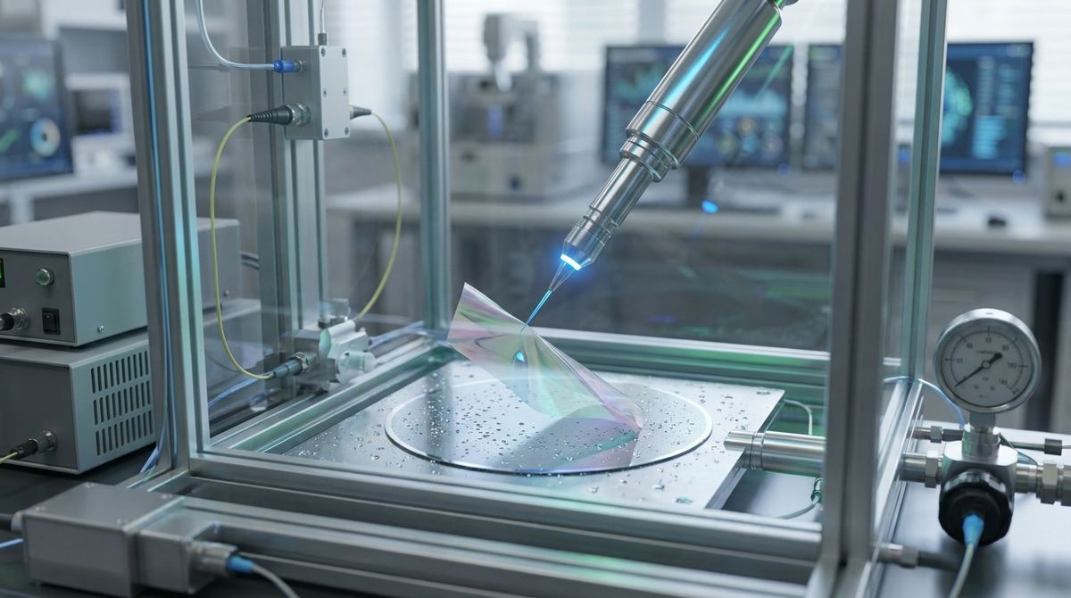
Imagine attempting to build a massive, high-tech skyscraper, but instead of using steel beams and concrete, you are working with single layers of atoms that are so thin they are invisible to the naked eye. If you place a single piece just one nanometer out of alignment, or if a tiny speck of dust gets trapped between layers, the entire structure becomes useless. For years, creating these ultra-thin, layered structures has been a slow, painstaking process performed by highly skilled scientists using microscopes and tiny tweezers. It is more of an art form than a scalable engineering process. This research represents the moment that art turns into automated science, moving us closer to a world where we can manufacture materials atom by atom with perfect consistency.
The field of two-dimensional materials, headlined by the superstar graphene, is currently hitting a significant manufacturing wall. While we know that stacking different 2D materials—like graphene, molybdenum disulfide, or hexagonal boron nitride—can create entirely new electronic properties, we cannot currently make these stacks reliably or quickly. This difficulty stems from several physical and logistical hurdles.
First, there is the issue of scale and throughput. Manual assembly, often called mechanical exfoliation and transfer, is incredibly slow. A researcher might spend hours or even days trying to stack just a few layers of material onto a substrate. This makes it nearly impossible to produce large quantities of these materials for industrial use. If we want to use these materials in consumer electronics, the process must be fast and repeatable.
Second, the precision required is staggering. When you stack two different 2D materials, they are held together by van der Waals forces, which are much weaker than the covalent bonds found in traditional silicon-based semiconductors. Because these forces are so delicate, the alignment between the crystal lattices of the two materials is critical. If the lattices are misaligned, it creates interfacial strain. This strain can distort the electronic band structure of the material, effectively changing its conductivity or its ability to act as a semiconductor. If a researcher is working manually, even a slight tremor or a momentary lapse in focus can ruin the electronic performance of the device.
Third, there is the problem of contamination and defects. When stacking layers by hand, it is almost impossible to prevent microscopic bubbles or trapped air from forming between the layers. These trapped particles act as scattering centers for electrons. When an electron traveling through a material hits a defect or a trapped bubble, its mobility is reduced, which slows down the device and generates heat. For the next generation of ultra-fast, low-power electronics, these defects must be eliminated through a level of cleanliness and control that human hands simply cannot provide.
The solution proposed by this research is a closed-loop, AI-driven robotic system. Instead of a human looking through a microscope and moving a lever, the system uses high-resolution cameras and advanced computer vision to see the materials. An artificial intelligence brain then analyzes these images in real-time, identifying the exact shape, size, and position of every tiny flake.
Once the AI understands what is happening on the sample surface, it sends precise instructions to a high-precision robotic arm. This robot operates on a scale much smaller than a human finger can manage, moving with nanometer-level accuracy. The system doesn't just follow a set of pre-programmed moves; it uses a feedback loop. This means the AI is constantly watching the robot work, checking to see if the flakes are aligning correctly, and making tiny, instantaneous corrections to ensure the stack is perfect. It is essentially a self-correcting machine that can "see" the atomic-scale landscape and manipulate it with superhuman precision.
The technical architecture of this system begins with the optical detection of the 2D materials. Even though many 2D materials are transparent, they interact with light in specific ways based on their thickness. Through a process involving optical contrast, a camera can capture the distinct edges and layers of a material like graphene or a transition metal dichalcogenide. The AI uses convolutional neural networks to process these visual inputs, distinguishing between the actual material flakes and the background substrate.
Once the AI has identified the target flakes, the motion planning algorithm takes over. This algorithm calculates the optimal trajectory for the robotic manipulator to pick up a flake and place it onto the target substrate. The robotic system typically utilizes piezoelectric actuators, which are components that move in incredibly small increments when an electric voltage is applied. This allows for the sub-nanometer positioning required to align crystal lattices.
The actual assembly process often involves a transfer method where a 2D flake is picked up using a polymer-coated stamp and then pressed onto another layer. As the layers make contact, the system manages the van der Waals interaction. The AI monitors the contact area to ensure that the flakes are making full contact without trapping air or contaminants. This is where the integration of sensing and action becomes vital. The system can detect the presence of "bubbles" or wrinkles in the material layer and can adjust the pressure or the alignment of the robotic arm to minimize these defects. By controlling the interface at the atomic level, the system ensures that the electronic pathways remain unobstructed, preserving the high carrier mobility that makes these materials so valuable.
The research, conducted by Xiaoxi Li, Jinkun He, Haojie Liu, Xipeng Liu, Zewen Wu, Jing Li, Kai Zhao, Shan Li, Xingdan Sun, Xiaoxue Fan, Zhiren Xiong, Xingguang Wu, et al., demonstrates that this automated approach significantly outperforms manual methods in several key metrics. The most immediate finding was a massive increase in throughput. By automating the identification and placement of flakes, the time required to create complex hetero-structures was reduced by orders of magnitude compared to manual labor.
Beyond speed, the researchers found that the AI-driven system provided a level of consistency that was previously unattainable. In manual assembly, the electronic properties of the resulting device can vary wildly from one sample to the next due to human error. The robotic system, however, produced devices with highly predictable and repeatable electronic characteristics. Because the alignment and contact area were controlled so tightly, the electrical conductivity and the bandgap characteristics remained consistent across multiple trials.
Furthermore, the researchers discovered that the AI could optimize the assembly process itself. Through iterative learning, the system can find the best way to stack specific combinations of materials to achieve a desired outcome. This opens the door to a new type of material discovery, where the machine is not just a tool for assembly, but an active participant in designing the specific architecture of a 2D hetero-assembly.
The implications of this research extend far beyond the walls of a physics laboratory. The ability to reliably create 2D hetero-assemblies is a fundamental requirement for the next era of semiconductor technology. Current silicon-based technology is approaching its physical limits as transistors get smaller and smaller. We are running into problems with heat dissipation and quantum tunneling that silicon simply cannot overcome.
2D materials offer a way out of this silicon bottleneck. Because they are atomically thin, they allow for much higher levels of electrostatic control in a transistor, meaning we can make devices that are faster and use much less power. By stacking different 2D materials, we can "engineer" the electronic properties of a device. For example, we could stack a layer that acts as a perfect conductor with a layer that acts as a high-performance semiconductor to create an ultra-efficient transistor.
The ability to automate this assembly means we are moving from the discovery phase of 2D materials into the engineering phase. We are transitioning from asking "what can these materials do?" to "how can we manufacture them for the market?" This transition is essential for the development of next-generation technologies, including ultra-sensitive chemical sensors, high-frequency communication devices for 6G networks, and even components for quantum computers.
Despite the impressive results, it is important to note that this technology is not yet a plug-and-play industrial manufacturing solution. The current system is a highly sophisticated laboratory tool designed for precision and discovery rather than mass production on a factory floor. There are several areas that require further development.
First, the throughput, while much higher than manual assembly, is still far below what is required for true industrial-scale manufacturing. To replace silicon, we would need to move from assembling a few flakes at a time to processing entire wafers of material simultaneously.
Second, the complexity of the material library is a challenge. While the system works well for common 2D materials like graphene and MoS2, a full-scale industrial process would need to handle a much wider variety of materials with different surface energies and mechanical properties. Each new material might require a different set of AI training data and robotic parameters.
Third, the environmental requirements for these assemblies are extremely strict. To achieve the highest performance, these processes often need to occur in ultra-high vacuum environments or inert gas environments to prevent oxidation and contamination. Integrating high-precision robotics and AI into a vacuum-sealed, cleanroom-compatible system adds a significant layer of engineering complexity.
The successful automation of 2D hetero-assemblies will likely impact several high-tech industries. In the realm of consumer electronics, we may see a new class of extremely thin and efficient processors that extend the battery life of smartphones and wearable devices significantly. The reduced power consumption is a direct result of the precise control over the electronic interfaces achieved by the robotic system.
In the field of sensing, these materials could lead to a new generation of bio-sensors. Because 2D materials have a very high surface-area-to-volume ratio, every atom is essentially on the surface, making them incredibly sensitive to their environment. An automated, precise manufacturing process would allow us to create arrays of these sensors for detecting single molecules of a virus or a specific chemical toxin in a medical diagnostic device.
Finally, in the burgeoning field of quantum computing, the ability to create perfectly aligned heterostructures is critical. Quantum bits, or qubits, are incredibly sensitive to noise and defects. The ability to use AI to place materials with atomic precision could help create the highly pure, defect-free environments required for stable quantum operations, potentially accelerating the timeline for practical quantum computers.
If you take away only one concept from this research, let it be this: the transition from manual craftsmanship to AI-driven robotic automation is the essential bridge that will carry 2D material science from a laboratory curiosity to a cornerstone of modern technology.
How does an AI see something that is only one atom thick?
The AI does not see the atoms directly, but it sees how the material affects light. When a 2D material is placed on a substrate, it causes a tiny change in how light reflects off that surface, a phenomenon known as optical contrast. The AI is trained to recognize these subtle changes in brightness and color to identify the material and its edges.
Why is it such a big deal to stack these materials?
Stacking different 2D materials allows us to create "designer" materials. By choosing which layers to stack, we can control the electrical, optical, and magnetic properties of the final structure. This is something you cannot easily do with traditional bulk materials, where the properties are fixed by the crystal structure of the entire block.
Can this technology replace human scientists in the lab?
It is more accurate to say that this technology augments human scientists. The robot handles the repetitive, high-precision, and error-prone tasks, freeing the researchers to focus on designing new materials and interpreting complex data. The AI handles the "how" of assembly, while the scientists handle the "why" and "what next."
Will this make computer chips much smaller?
Yes, potentially. Because 2D materials are incredibly thin, they allow for much tighter control over the flow of electricity in a transistor. This could allow us to continue shrinking components beyond the limits of current silicon technology, leading to even faster and more efficient electronics.
Is the technology ready for mass production today?
No, not yet. Currently, this is a cutting-edge research tool used in laboratories to explore new possibilities. Moving from this high-precision, low-volume assembly to a massive-scale industrial process is the next major engineering challenge for the industry.
The research presented by Xiaoxi Li and the team represents a pivotal shift in materials science. By integrating artificial intelligence with high-precision robotics, they have provided a roadmap for overcoming the most significant barrier in 2D material research: the assembly problem. As we move toward a future where electronics are defined by the precise arrangement of individual atomic layers, the tools developed in this study will be the foundation upon which the next generation of technological breakthroughs is built. The marriage of AI and robotics is not just making the process faster; it is making the impossible—the perfect assembly of the world's thinnest materials—attainable.
Serious about B2B integration? Test our premium Pulsed Electrical Resistive Carbon Heating turbostratic graphene in your lab. 100g sample packs available now.
Explore More
Researchers discover a moiré heterostructure with a unique "dual-flatness" electronic property, enabling continuous electrical tuning between exotic quantum...

Explore chiral fermion localization in two-kink systems. This theoretical physics research offers a powerful new model for controlling electrons in...

Explore how a gate-defined graphene superlattice can create a versatile quantum sensor, leveraging unique electron states for advanced magnetic field detection.