
Controlled Loop Expansion for the Topological Heavy Fermion Model
New research introduces a controlled loop expansion for the topological heavy fermion model, a powerful theoretical tool for designing future quantum materials.
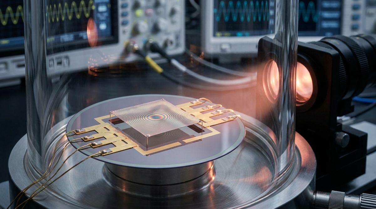
Standard semiconductor-based detectors, such as photodiodes, rely on the generation of electron-hole pairs when photons strike the material. While effective for visible light, this mechanism becomes inefficient in the Terahertz (THz) and far-infrared (FIR) spectrum because the photon energy is often too low to overcome the bandgap of conventional semiconductors. This leads to low responsivity and high noise floors in the long-wavelength regime.
A new approach utilizes the physics of correlated insulators. In magic-angle twisted bilayer graphene (MATBG), the electronic structure is modified by the moiré pattern created by the slight twist between the two graphene layers. At a specific twist angle, the electronic bands become nearly flat, leading to strong electron-electron interactions that can turn the material into a correlated insulator.
Instead of using light to create new charge carriers, we can use long-wavelength radiation to heat the existing electronic subsystem. Because the electronic heat capacity is significantly lower than the lattice heat capacity at cryogenic temperatures, even a tiny amount of absorbed power causes a massive change in the electronic temperature. This triggers an insulator-to-metal transition, resulting in a giant, measurable change in electrical resistance. This guide outlines how to prototype a bolometer based on this principle.
The device operates on a principle distinct from standard photodetectors. In a typical photodiode, the signal is proportional to the number of photons that create carriers. In a moiré bolometer, the signal is proportional to the change in resistance caused by the heating of the electron gas.
When the graphene is tuned to the half-filling point of the moiré band, it enters a correlated insulating state with a distinct energy gap. When long-wavelength photons (with energies comparable to the flat-band width) are absorbed, they selectively heat the electrons without significantly heating the crystal lattice. This electronic heating suppresses the many-body correlation that maintains the insulating state, effectively melting the insulator into a metal.
The resulting voltage responsivity is exceptionally high, potentially exceeding millivolts per nanowatt of absorbed power. This makes the device capable of detecting extremely faint radiation that would be invisible to traditional sensors.
The primary application for this technology is in the field of high-sensitivity Terahertz spectroscopy and sensing. Because the response is broadband and relies on heating rather than carrier generation, it is not limited by the bandgap constraints that plague traditional materials.
Potential use cases include:
• Remote sensing for non-destructive inspection of materials.
• High-speed, low-noise imaging in the far-infrared spectrum.
• Security scanning for detecting low-energy radiation signatures.
• Laboratory-scale research into many-body quantum phenomena.
Building a prototype requires high-precision nanofabrication tools and cryogenic environments.
Materials:
• High-quality monolayer graphene flakes (exfoliated or high-quality CVD).
• Hexagonal Boron Nitride (HBN) flakes (used for encapsulation to ensure high carrier mobility).
• Substrate: Silicon with a thick thermal oxide layer (SiO2/Si).
• Metal for contacts: Titanium (Ti) for adhesion and Gold (Au) for conductivity.
• Resist: PMMA or Polycarbonate for the dry transfer process.
Equipment:
• Optical microscope and Scanning Electron Microscope (SEM).
• Electron Beam Lithography (EBL) system for precise electrode patterning.
• Thermal evaporation or sputtering system for metal deposition.
• Cryogenic probe station or a Liquid Helium-cooled cryostat.
• High-precision DC voltage source and a Lock-in amplifier (e.g., SR830) for signal extraction.
• Rotation stage with sub-degree precision (for the twist angle control).
The success of this device depends entirely on the precision of the twist angle and the quality of the encapsulation.
1. Substrate Preparation: Clean the SiO2/Si substrate using standard solvent cleaning (Acetone, IPA) followed by oxygen plasma treatment to ensure a pristine surface for flake transfer.
2. The Moiré Stack Assembly: This is the most critical step. Using a dry transfer method (such as a PC/PDMS stamp), you must stack the layers in the following order: HBN (bottom) / Graphene / Graphene / HBN (top).
3. Twist Angle Control: To achieve the magic angle, the top graphene layer must be rotated relative to the bottom layer. While the exact angle depends on the specific graphene quality, the target is approximately 1.1 degrees. We assume a tolerance of +/- 0.05 degrees. This requires a high-precision rotation stage during the transfer process.
4. Electrode Patterning: Use Electron Beam Lithography to define the contact pads and the channel area. The channel should be small (micrometer scale) to minimize the total heat capacity and maximize the temperature rise from absorbed radiation.
5. Metal Deposition: Deposit a thin layer of Titanium followed by a thicker layer of Gold via thermal evaporation. This ensures low contact resistance, which is vital for measuring the small resistance changes during the transition.
6. Device Tuning (Gate Optimization): Once the device is fabricated, it must be tuned to the half-filling point. This is achieved by applying a back-gate voltage (via the Si substrate) or a top-gate voltage (if using a dual-gated setup). You must sweep the gate voltage while monitoring the resistance at cryogenic temperatures to identify the insulating state.
Once the device is tuned to the correlated insulating state, follow this testing plan:
1. Resistance-Temperature (R-T) Characterization: Measure the resistance of the device while slowly sweeping the temperature from 4K to 50K. You should observe a sharp increase in resistance as the temperature drops, signaling the onset of the correlated insulating state.
2. Responsivity Measurement: Apply a known, low-power long-wavelength radiation source (such as a THz source or a far-IR lamp) to the device. Measure the resulting voltage change (ΔV) across the device.
3. Calculation: Calculate the responsivity (R) using the formula: R = ΔV / P, where P is the absorbed power. For a successful prototype, the responsivity should be in the millivolt-per-nanowatt range.
4. Noise Floor Analysis: Measure the voltage noise (V_noise) in the absence of radiation to determine the minimum detectable power (MDP).
• Twist Angle Deviation: If the angle is not near 1.1 degrees, the flat bands will not form, and the correlated insulator state will not appear.
Mitigation: Use Raman spectroscopy to verify the twist angle across the device area before proceeding to electrode fabrication.
• Thermal Leakage: If the device is too large or the substrate is too conductive, the heat from the photons will dissipate into the lattice before it can heat the electrons.
Mitigation: Keep the device channel dimensions in the sub-micron to low-micron range and use HBN encapsulation to decouple the electronic system from the substrate.
• Contact Resistance: High contact resistance can mask the resistance change of the graphene channel.
Mitigation: Use EBL for precise contact placement and ensure the metal-graphene interface is cleaned via plasma before deposition.
• Temperature Control: The correlated state is highly sensitive to temperature.
Mitigation: All testing must be performed in a stable cryogenic environment (ideally < 10K) to maintain the insulating state.
This guide is based on the research findings published by Elesin et al. (2026) regarding the "Correlated Insulator Moiré Bolometer." The specific mechanism described—the use of weak, long-wavelength photons to heat the electronic subsystem and suppress the many-body correlated gap—is the core engineering principle for this device. The reported responsivity of >1 mV/nW and the robustness of the effect in magnetic fields are the performance benchmarks for this prototype.
Serious about B2B integration? Test our premium Pulsed Electrical Resistive Carbon Heating turbostratic graphene in your lab. 100g sample packs available now.
Explore More
New research introduces a controlled loop expansion for the topological heavy fermion model, a powerful theoretical tool for designing future quantum materials.

Researchers derived an analytic formula for twisted bilayer graphene electron lifetimes, providing a key design tool for future quantum and electronic devices.

Learn to build a high-responsivity 1.5 µm graphene photodetector. This guide details the materials and steps for a prototype based on upconversion...